Driving method of display panel and display device utilizing the method

A technology of display panel and driving method, which is applied to static indicators, instruments, etc., and can solve problems such as uneven brightness

Active Publication Date: 2011-09-21
AU OPTRONICS CORP
View PDF9 Cites 4 Cited by
  • Summary
  • Abstract
  • Description
  • Claims
  • Application Information

AI Technical Summary

Problems solved by technology

[0010] The purpose of the present invention is to provide a method for driving a display panel, whic...

Method used


Image

  • Driving method of display panel and display device utilizing the method
  • Driving method of display panel and display device utilizing the method
  • Driving method of display panel and display device utilizing the method

Examples


no. 1 example

[0061] In the display panel of this example, all the pixels are electrically coupled in a traditional manner, that is, the pixels electrically coupled to the K scan line are located in the same column, where K is a natural number.

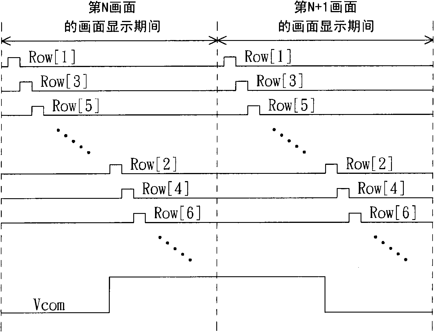
[0062] Figure 6 It is an explanatory diagram of a driving method of a display panel according to an embodiment of the present invention. exist Figure 6 Among them, the marks Row[1], Row[3] and Row[5] represent the gate signals corresponding to the pixels in the first column, the third column and the fifth column respectively, and the marks Row[2], Row[4] and Row[6] respectively represent the gate signals corresponding to the pixels in the second column, the pixels in the fourth column and the pixels in the sixth column, and the marks Vcom_Cst[1], Vcom_Cst[3] and Vcom_Cst[5] respectively represent the pixels in the first column, The common potentials corresponding to the pixels in the third column and the pixels in the fifth column, and the mark...

no. 2 example

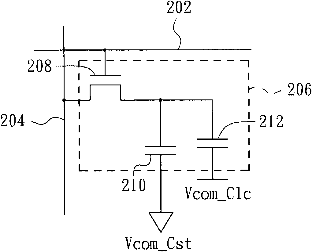
[0068] This example is mainly to illustrate Figure 6 The described driving method can also be applied to different pixel architectures to Figure 8 to explain. Figure 8 It is a schematic diagram of a pixel structure of a display panel. exist Figure 8 Among them, mark 802 represents a pixel, marks 811-816 represent data lines, marks Row[m-1], Row[m] and Row[m+1] represent scan lines, wherein m is a natural number, and marks Vcom_Cst[ m] is represented as a common electrode corresponding to the scanning line Row[m]. Depend on Figure 6 It can be seen that the pixels of the display panel are electrically coupled to the scanning lines in a zigzag manner, so that any two adjacent pixels on the same scanning line are located in different columns.

[0069] Implemented under this pixel architecture Figure 6 The driving method shown can make the display panel achieve the effect of dot inversion. In this way, this effect can be used to average the visual perception and furthe...

no. 3 example

[0071] This embodiment mainly illustrates that the scanning lines of the display panel described in the first embodiment can also be divided into more groups for driving, so as to Figure 9 to explain.

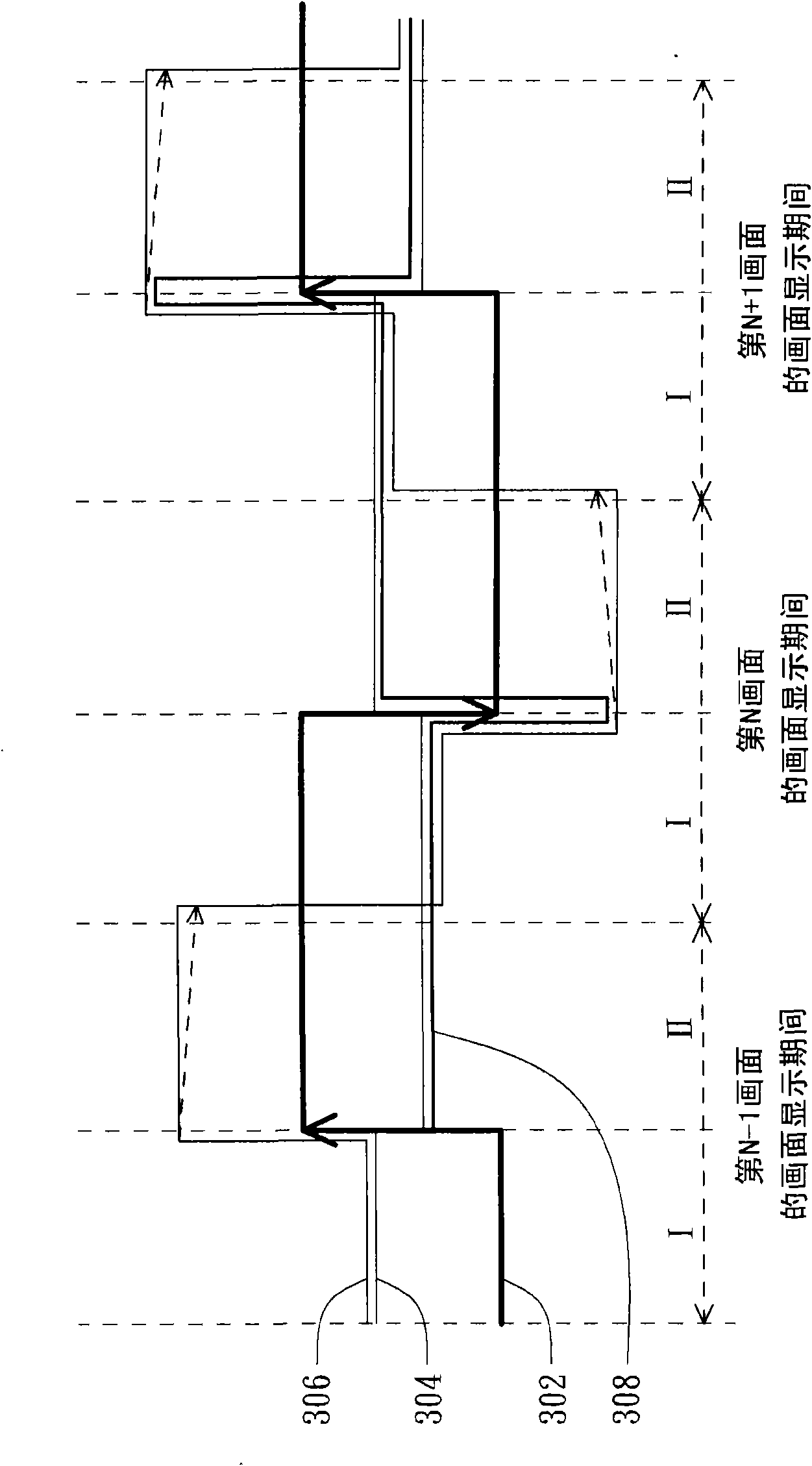
[0072] Figure 9 It is an explanatory diagram of a driving method of a display panel according to another embodiment of the present invention. exist Figure 9 Among them, the labels Row[1], Row[3], Row[5] and Row[7] respectively represent the gate signals corresponding to the pixels in the first column, the pixels in the third column, the pixels in the fifth column and the pixels in the seventh column, The marks Row[2], Row[4], Row[6] and Row[8] respectively represent the second row of pixels, the fourth row of pixels, the sixth row of pixels and the corresponding gate signals, and the marks Vcom_Cst[1], Vcom_Cst[3], Vcom_Cst[5], and Vcom_Cst[7] represent the common potentials corresponding to the pixels in the first column, the third column, the fifth column, and the seven...


PUM


Abstract

The present invention provides a driving method of a display panel and a display device utilizing the method. The display panel is provided with the following components: a plurality of pixels, a plurality of data wires, a plurality of scanning wires and a plurality of common electrodes. The pixels are arranged in a matrix. The data wires and the scanning wires are electrically coupled with the pixels. Furthermore the common electrodes are all provided in the lower substrate of the display panel. The driving method comprises the following steps: providing a plurality of common levels with different time sequences to the common electrodes, wherein each common level is provided with two reference levels; and providing a plurality of grid signals with different time sequences for the scanning wires in one picture display period for starting the pixel, and switching to a reference level of the common level which corresponds with the pixel to be opened before starting the pixel.

Description

【Technical field】 [0001] The present invention relates to the field of display technology, and in particular relates to a driving method of a display panel and a display device using the method. 【Background technique】 [0002] In the traditional column inversion (rowinversion) driving technology, most of the odd-numbered scan lines in the display panel are driven sequentially, and then the even-numbered scan lines are sequentially driven, and the upper substrate of the display panel (ie, The color filter substrate) and the lower substrate (that is, the thin film transistor array substrate) both adopt the same common potential. figure 1 It is a schematic diagram of the timing sequence of the gate signal and the timing sequence of the common potential adopted in this driving technology. exist figure 1 Among them, the marks Row[1], Row[3] and Row[5] represent the gate signals corresponding to the pixels in the first column, the third column and the fifth column respectively, ...

Claims


Application Information

Patent Timeline
IPC IPC(8): G09G3/20
Inventor 白承丘
Owner AU OPTRONICS CORP
Why Eureka
Try Eureka