Optically-functional film and method of manufacturing the same, display and method of manufacturing the same
An optical function and display technology, which is applied in optics, optical components, semiconductor/solid-state device manufacturing, etc., can solve problems such as color imbalance, EL light-emitting high directivity, viewing angle brightness reduction, etc., to prevent moisture diffusion and prevent brightness The effect of reducing and preventing deterioration
- Summary
- Abstract
- Description
- Claims
- Application Information
AI Technical Summary
Problems solved by technology
Method used
Image
Examples
no. 1 approach
[0049] 1. First Embodiment (Example of Disposing an Optical Functional Film on the Surface of an Organic Light-Emitting Element)
[0050] 2. Second embodiment (example of disposing an optical functional film on a sealing panel)
[0051] 3. Application examples (application examples of displays and optical functional films)
[0052] first embodiment
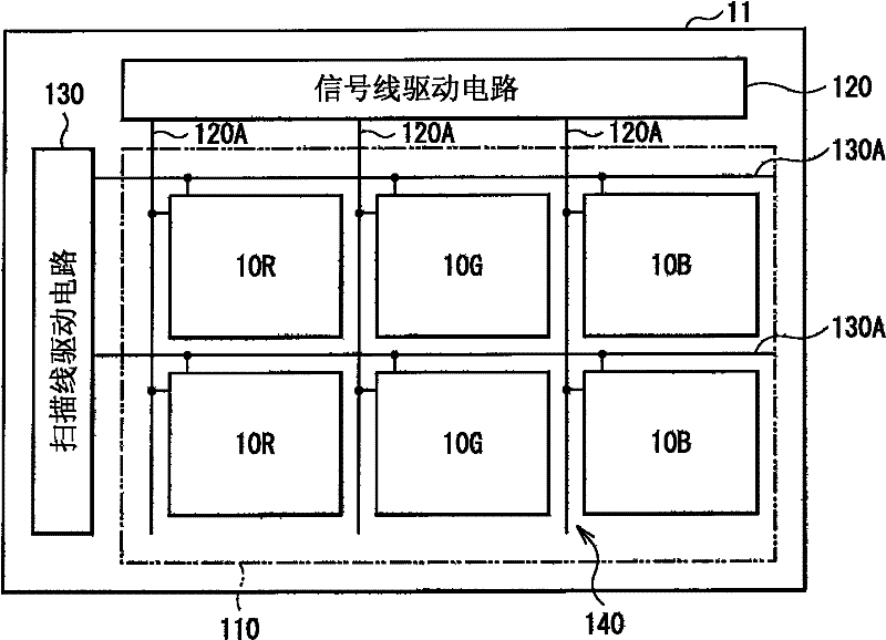
[0053] figure 1 The configuration of the display according to the first embodiment of the present invention is shown. This display is used as an organic EL television or the like, and in this display, for example, a plurality of organic light emitting elements 10R, 10G, and 10B (to be described later) are arranged in a matrix form on a substrate 11 as a display area 110 . A signal line driver circuit 120 and a scan line driver circuit 130 as drivers (for screen display) are arranged around the display area 110 .
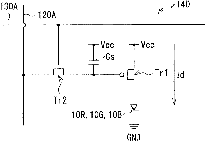
[0054] The pixel driving circuit 140 is arranged in the display area 110 . figure 2 An example of a pixel drivin...
no. 2 approach
[0122] Figure 20 The cross-sectional configuration of the display area 110 in the display according to the second embodiment of the present invention is shown. This display has the same configuration as that of the first embodiment except that the optical functional film 20 is disposed on the adhesive layer 40 side of the sealing panel 30 . Therefore, in the following description, the same components are denoted by the same reference numerals as those of the first embodiment.
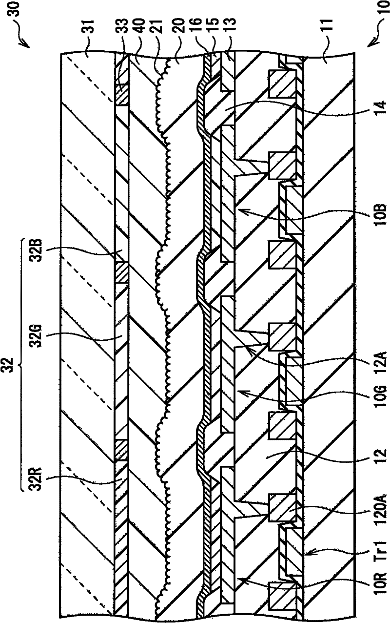
[0123] As in the case of the first embodiment, the display panel 10 includes the organic light emitting elements 10R, 10G, and 10B on the substrate 11 . The organic light emitting elements 10R, 10G, and 10B are covered with a protective film 17 made of silicon nitride or silicon oxide, if necessary.
[0124] The optical functional film 20 has the same configuration as that of the first embodiment except that the optical functional film 20 is disposed on the color filter 32 and the light shielding fil...
PUM
| Property | Measurement | Unit |
|---|---|---|
| thickness | aaaaa | aaaaa |
| thickness | aaaaa | aaaaa |
| refractive index | aaaaa | aaaaa |
Abstract
Description
Claims
Application Information


