Wiring structure of induction layer
A wiring structure and sensing layer technology, which is applied in the field of wiring structure of a single-layer sensing layer, can solve the problems of difficult detection of touch edge coordinates and small edge sensing area, and achieve the effects of easy edge coordinates, easy detection, and increased sensing area
- Summary
- Abstract
- Description
- Claims
- Application Information
AI Technical Summary
Problems solved by technology
Method used
Image
Examples
Embodiment Construction
[0010] The present invention will be further described below in conjunction with the accompanying drawings and embodiments.
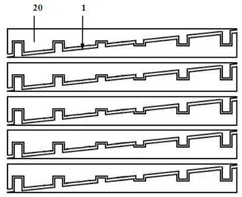
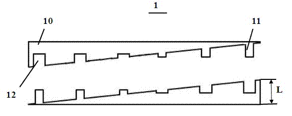
[0011] Please refer to figure 1 and figure 2 , the wiring structure of the sensing layer involved in the present invention, the sensing layer includes a plurality of vertically arranged touch electrode groups 1, and the touch electrode group 1 includes two opposing touch electrodes 20, that is, one of the touch electrodes 20 is rotated 180 degrees clockwise relative to the other touch electrode 20 . The opposite edges of the two touch electrodes 20 in the touch electrode group 1 are facing edges.
[0012] The touch electrode 20 includes a main body 10 , the longitudinal width L of the main body 10 gradually decreases from one end to the other end, and the shape of the main body 10 may be a triangle, a trapezoid or other figures whose longitudinal width gradually decreases from one end to the other end. The main body 10 is provided with at least one ...
PUM
 Abstract
Description
Claims
Application Information


