

Carbon nanometer tube/silicon honeycomb array preparing method
A technology of carbon nanotubes and arrays, which is applied in the field of preparation of nano-functional materials, and can solve the problems of low sensitivity, nonlinear response, and low emission current density of carbon nanotube-based humidity sensors.
- Summary
- Abstract
- Description
- Claims
- Application Information
AI Technical Summary
Problems solved by technology
Method used
Image

Examples
Embodiment 1
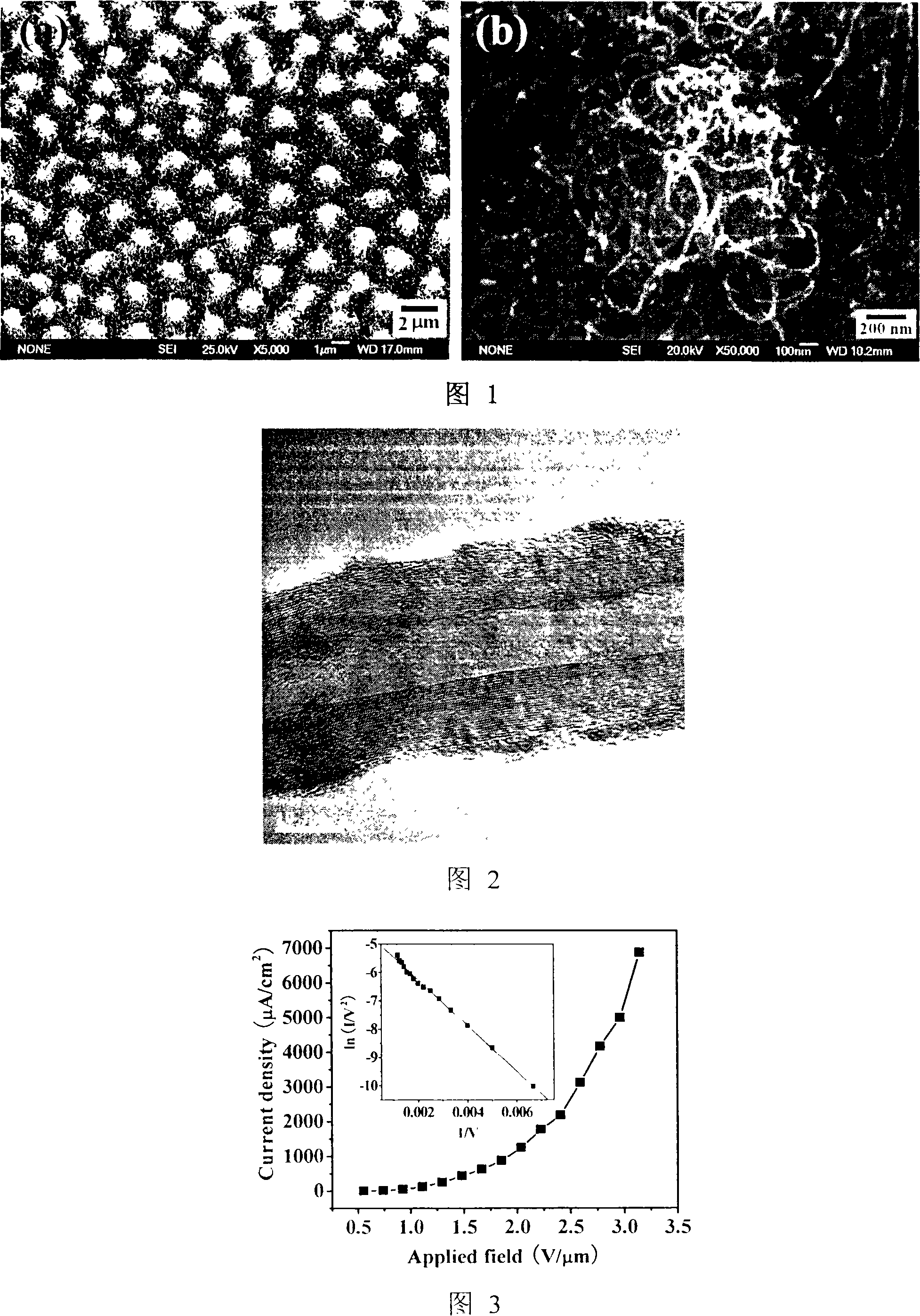
[0023] 1. Put a P-type (111) single crystal silicon wafer with a resistivity of 0.015Ω·cm into the autoclave, and fill it with an etching solution composed of hydrofluoric acid with a concentration of 13.00mol / l and ferric nitrate solution with a concentration of 0.04mol / l , the solution volume filling degree of the autoclave is 80%, corroded at a temperature of 140° C. for 60 minutes, and the substrate material silicon nanoporous column array (Si-NPA) is prepared;
[0024] 2. Put the Si-NPA substrate into a horizontal tube furnace, raise it to 700°C under the protection of 60sccm nitrogen, keep the temperature constant, and change the gas to N 2 :H 2 =60sccm: the carrier gas of 30sccm, the xylene solution that will be dissolved with 0.015mol / l ferrocene is sent in the furnace with the speed of 0.2mol / l at the same time, after reacting 15min, solution stops conveying, under the protection of nitrogen, the temperature in the furnace is lowered. to room temperature. That is, a...
Embodiment 2
[0026] 1. Put a P-type (111) single crystal silicon chip with a resistivity of 0.2Ω·cm into the autoclave, and fill it with an etching solution composed of hydrofluoric acid with a concentration of 10.00mol / l and a ferric nitrate solution of 0.06mol / l , the solution volume filling degree of the autoclave is 85%, corroded at a temperature of 180° C. for 55 minutes, and the substrate material silicon nanoporous column array (Si-NPA) is prepared;
[0027] 2. Put the Si-NPA substrate into a horizontal tube furnace, raise it to 800°C under the protection of 60 sccm (standard cubic centimeter per minute) argon, keep the temperature constant, and change the gas to Ar:H 2 =50sccm: 40sccm carrier gas, at the same time, the ethylenediamine solution dissolved with 0.03mol / l nickelocene is sent to the furnace at a speed of 0.3mol / l, and the solution stops transporting after 10 minutes of reaction, and the temperature in the furnace is lowered under the protection of nitrogen. Bring to roo...
Embodiment 3
[0029] 1. Put a P-type (111) single crystal silicon wafer with a resistivity of 0.05Ω·cm into the autoclave, and fill it with an etching solution composed of hydrofluoric acid with a concentration of 8.00mol / l and ferric nitrate solution with a concentration of 0.08mol / l. , the solution volume filling degree of the autoclave is 88%, corroded at a temperature of 100° C. for 80 minutes, and the substrate material silicon nanoporous column array (Si-NPA) is prepared;
[0030] 2. Put the Si-NPA substrate into a horizontal tube furnace, raise it to 900°C under the protection of 60 sccm (standard cubic centimeter per minute) nitrogen, keep the temperature constant, and change the gas to N 2 :H 2 =40sccm: the carrier gas of 50sccm, simultaneously the toluene solution that will be dissolved with 0.02mol / l ferrocene and 0.02mol / l ferrocene cobalt is sent in the furnace with the speed of 0.4mol / l, after reaction 8min, solution stops conveying, nitrogen gas Under protection, the tempera...
PUM
| Property | Measurement | Unit |
|---|---|---|
| Resistivity | aaaaa | aaaaa |
| Current density | aaaaa | aaaaa |
| Resistivity | aaaaa | aaaaa |
Abstract
Description
Claims
Application Information