Field emission lighting device

a field emission and lighting device technology, applied in the direction of discharge tube/lamp details, discharge tube luminescnet screens, discharge tube main electrodes, etc., can solve the problems of increasing power consumption and complexity of configuration of hid lamps, inability to provide high light brightness and uniformity, and inability to achieve high light brightness and uniformity, and improve the effect of field emission capability

Inactive Publication Date: 2006-09-07
HON HAI PRECISION IND CO LTD
View PDF11 Cites 5 Cited by
  • Summary
  • Abstract
  • Description
  • Claims
  • Application Information

AI Technical Summary

Benefits of technology

[0012] The combined emitter tip and the emitter base have good mechanical strength, and excellent field-emission capability. In addition, the isolating layer provides a stable substrate for supporting the emitter bases and the emitter tips, thereby enhancing stability thereof and increasing working lifetime thereof. As such, the combined emitter tip and the emitter base may operate under desired high voltage electrical fields without the risk of being damaged and thereby providing a high luminous efficiency and a satisfactory brightness at a long period of time.

Problems solved by technology

This increases power consumption and complexity of configuration of the HID lamp.
Nevertheless, all of the above-mentioned light sources have a common shortcoming that they cannot provide a high light brightness and uniformity.
Therefore, energy consumption is undesirably increased accordingly.

Method used


Image

  • Field emission lighting device
  • Field emission lighting device
  • Field emission lighting device

Examples


Embodiment Construction

[0020] Embodiments of the present invention will now be described in detail below and with reference to the drawings.

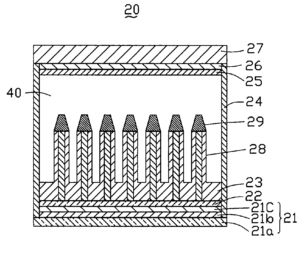
[0021] Referring to FIG. 1, this illustrates a field emission lighting device 10 in accordance with a first preferred embodiment of the present invention. The field emission lighting device 10 mainly includes a low substrate 11a, a cathode 11b, a nucleation layer 12, an isolating layer 13, a fluorescence layer 15, a light-permeable anode 16, a transparent upper substrate 17, a plurality of isolating emitter bases 18, and a plurality of emitter tips 19.

[0022] The nucleation layer 12 is located between the cathode 11b and the isolating layer 13. The isolating layer 13 is formed on the nucleation layer 12. The isolating emitter bases 18 are formed on the isolating layer 13. The emitter tips 19 each are formed on a respective isolating emitter base 18. The anode 16 is formed on an interior surface of the upper substrate 17. The fluorescence layer 15 is formed on the ano...


PUM


Abstract

A field emission lighting device is disclosed in the present invention. The field emission lighting device includes a cathode, an isolating layer, a plurality of isolating emitter bases, a plurality of niobium emitter tips each formed on a respective emitter base, a light-permeable anode disposed opposite to the cathode, and a fluorescence layer formed on the anode. The isolating layer is formed on the cathode. The isolating emitter bases extend from the isolating layer. The isolating layer and the isolating emitter bases are comprised of diamond like carbon. The isolating emitter bases each include an electrically conductive connecting portion configured for establishing an electrically conductive connection between the emitter tip and the cathode.

Description

CROSS-REFERENCES TO RELATED APPLICATION [0001] This application is related to a copending U.S. patent application filed on Jul. 29, 2005, entitled “FIELD EMISSION LIGHTING DEVICE”, and another copending U.S. patent application filed on Nov. 23, 2005, entitled “A BACKLIGHT DEVICE USING A FIELD EMISSION LIGHT SOURCE”, each having the same assignee as the instant application. The disclosures of the above-identified applications are incorporated herein by reference.FIELD OF THE INVENTION [0002] The present invention relates to electronic lighting techniques, and more particularly to a field emission lighting device. DESCRIPTION OF RELATED ART [0003] Conventional light sources generally include combustion-based light sources, incandescent light sources, and fluorescent light sources. The fluorescent light sources include for example, high-intensity discharge (HID) lamps, and light emitting diode (LED) lamps. [0004] As regards a typical HID lamp, a low voltage has to be converted into a h...

Claims


Application Information

Patent Timeline
Patent Type & Authority Applications(United States)
IPC IPC(8): H01J1/02H01J1/00
CPCH01J63/06
Inventor CHEN, GA-LANE
Owner HON HAI PRECISION IND CO LTD
Why Eureka
Try Eureka