

Device monitoring method during semiconductor process
A device monitoring and semiconductor technology, applied in semiconductor/solid-state device testing/measurement, electrical components, circuits, etc., can solve the problems of inability to inspect wafers, low monitoring frequency, and risk expansion, and minimize potential risks.
- Summary
- Abstract
- Description
- Claims
- Application Information
AI Technical Summary
Problems solved by technology
Method used
Image

Examples
Embodiment Construction
[0026] The present invention will be further described below in conjunction with the accompanying drawings and specific embodiments, but not as a limitation of the present invention.
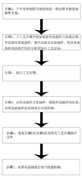
[0027] Such as figure 1 The device monitoring method in a semiconductor manufacturing process shown in the present invention includes the following steps:
[0028] Step a, formulating a sampling plan with a fixed number of samples before the start of the semiconductor manufacturing process;
[0029] Step b. Determine which wafers need to be sampled and which wafers do not need to be sampled according to the sampling plan before the start of the process steps, and evenly distribute the wafers that need to be sampled to each process equipment;
[0030] Step c, performing the process steps;
[0031] Step d, sampling with a sampling plan, and performing online detection on the sampled wafers according to the sampling results;
[0032] Step e, repeating step b to step d until all process steps are...
PUM
 Abstract
Description
Claims
Application Information