Charged coupled device module and method of manufacturing the same

A manufacturing method and module technology, applied in the fields of printed circuit manufacturing, semiconductor/solid-state device manufacturing, radiation control devices, etc., capable of solving problems such as easy fracture, easy deformation of the main circuit board 14, and affecting electrical connection properties, etc. To achieve the effect of improving the pin breakage

Inactive Publication Date: 2012-07-04
ALTEK CORP
View PDF6 Cites 2 Cited by
  • Summary
  • Abstract
  • Description
  • Claims
  • Application Information

AI Technical Summary

Problems solved by technology

[0003] However, since the CCD assembly 12 will be calibrated before it is fixed on the lens assembly 11, there may be an offset and/or gap between the CCD assembly 12 and the main circuit board 14. When the CCD assembly 12 is locked into the main circuit board 14 , its

Method used


Image

  • Charged coupled device module and method of manufacturing the same
  • Charged coupled device module and method of manufacturing the same
  • Charged coupled device module and method of manufacturing the same

Examples


Embodiment Construction

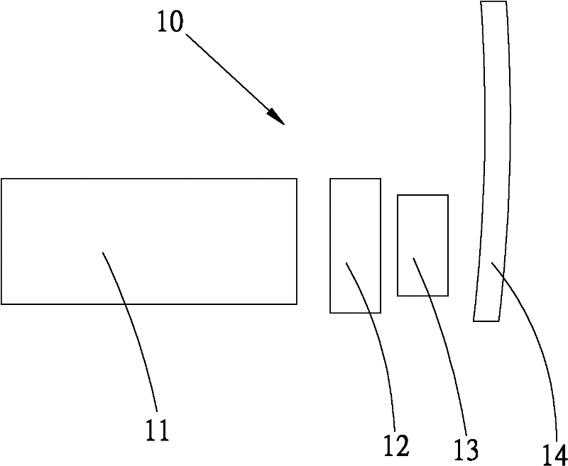
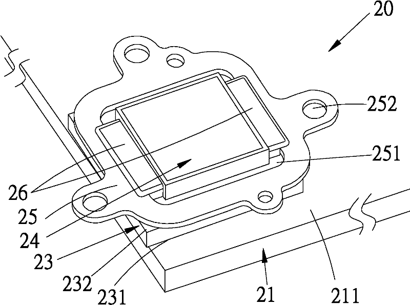
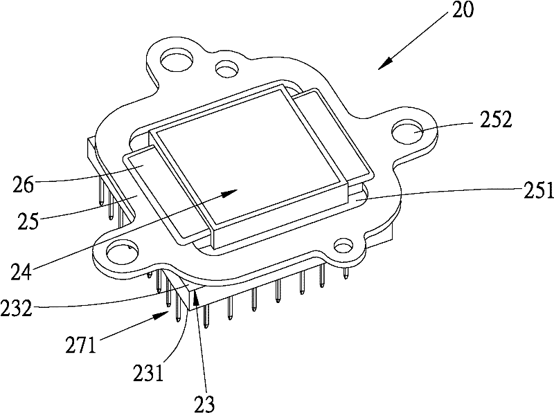
[0049] The CCD module and its manufacturing method of the present invention will be described below with reference to related drawings, wherein the same elements will be described with the same symbols. At the same time, the following diagrams are used to express schematic representations related to the features of the present invention. figure 2 It is a schematic diagram of the CCD module of the present invention. The CCD module 20 of the present invention is fixed between a lens assembly (not shown) and a main circuit board 21 , wherein the main circuit board 21 has a first board surface 211 .

[0050] And the CCD module 20 of the present invention includes a rigid circuit board 23 and a CCD element 24, wherein the rigid circuit board 23 has a first surface 231 and a second surface 232, and the first surface 231 of the rigid circuit board 23 is facing the main circuit The first board surface 211 of the board 21; and the CCD element 24 is disposed on the second surface 232 ...


PUM


Abstract

mbly and a main board having a first plate surface is disclosed. The CCD module comprises a hard PCB having a first surface and a second surface, a CCD component, and at least one fixed member. The first surface of the hard PCB faces the first plate surface of the main board. The CCD component facing the lens assembly is located on the second surface of the hard PCB. The fixed member is used for combining the hard PCB and the main board. The hard PCB and the fixed member can be used as a buffer to reduce possible damages to the CCD component and/or the main board.

Description

technical field [0001] The invention relates to a CCD module and its manufacturing method, in particular to a CCD module capable of improving the connection with a main circuit board and its manufacturing method. Background technique [0002] figure 1 An exploded schematic diagram showing a lens module of an existing imaging device. The existing lens module 10 at least includes a lens assembly 11 , a CCD assembly 12 and a main circuit board 14 . During assembly, the CCD assembly 12 will be fixed (such as: locked) on the lens assembly 11 first, and then surface mount technology (Surface Mount Technology, SMT) or dual in-linepackage (Dual in-linepackage, DIP) is used subsequently, and then The pins (not shown) of the CCD assembly 12 are then fixed to the main circuit board 14 . [0003] However, since the CCD assembly 12 will be calibrated before being fixed on the lens assembly 11, there may be an offset and / or gap between the CCD assembly 12 and the main circuit board 14....

Claims


Application Information

Patent Timeline
IPC IPC(8): H01L27/148H01L21/50H01L21/60
CPCH05K1/141H05K3/306H05K2201/049H05K2203/081H05K2203/167H05K2201/10151H05K2201/10303H01L27/14618H05K3/3494H01L2924/0002
Inventor 林资智
Owner ALTEK CORP
Why Eureka
Try Eureka