Liquid crystal display device and manufacturing method thereof

A technology of a liquid crystal display device and a manufacturing method, which is applied in the fields of optics, instruments, nonlinear optics, etc., and can solve problems such as degradation and disturbance of voltage response characteristics

Active Publication Date: 2016-05-18
SONY CORP
View PDF8 Cites 0 Cited by
  • Summary
  • Abstract
  • Description
  • Claims
  • Application Information

AI Technical Summary

Problems solved by technology

However, since the liquid crystal molecules aligned in the vertical direction are random to the direction in which the substrate falls, the disturbance of the orientation of the liquid crystal molecules due to the application of the voltage is a cause of deterioration of the response characteristics with respect to the voltage.

Method used


Image

  • Liquid crystal display device and manufacturing method thereof
  • Liquid crystal display device and manufacturing method thereof
  • Liquid crystal display device and manufacturing method thereof

Examples


Embodiment approach 1

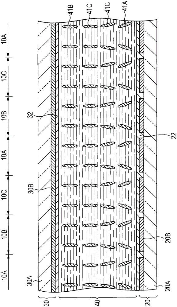
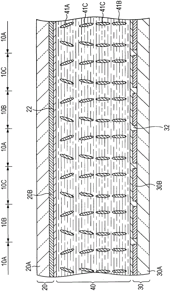
[0123] Embodiment 1 relates to a VA-mode liquid crystal display device (or liquid crystal display element) according to the first embodiment of the present invention and relates to a liquid crystal display device (or liquid crystal display element) according to the first embodiment or the third embodiment of the present invention. Production method. In Embodiment 1, the first alignment film 22 includes a compound obtained by crosslinking or polymerizing a polymer compound (compound before alignment treatment) having a crosslinkable functional group or a polymerizable functional group as a side chain (compound after alignment treatment); The second alignment film 32 includes the same compound as the compound constituting the first alignment film. That is, the first alignment film 22 and the second alignment film 32 are composed of the same polymer compound. In addition, the pretilt is imparted on the liquid crystal molecules by cross-linked or polymerized compounds. Here, aft...

Embodiment approach 2

[0246] Embodiment 2 is a modified example of Embodiment 1. FIG. In the liquid crystal display device of Embodiment 2, the first alignment regulation portion 21 is provided on the first electrode (pixel electrode) 20B, and the first alignment film 22 covers the first electrode (pixel electrode) 20B, the first alignment regulation portion 21 and the opposite surface of the first substrate (TFT substrate) 20. A schematic partial cross-sectional view of a liquid crystal display device according to Embodiment 2 of the present invention is shown in Figure 8 middle.

[0247] More specifically, the first slit portion 21 (portion on which no electrode is formed) having a striped or V-shaped pattern is provided, for example, in each pixel of the pixel electrode 20B. Here, an arrangement diagram of the first electrode (pixel electrode) 20B and the first slit portion 21 when the pixel is viewed from above is shown in Figure 10A with 10B middle. Thus, when a driving voltage is appli...

Embodiment approach 3

[0262] Embodiment 3 relates to the liquid crystal display device according to the second embodiment of the present invention, and relates to the manufacturing method of the liquid crystal display device according to the second embodiment and the third embodiment of the present invention.

[0263] In Embodiment 1, the compound after alignment treatment is obtained by crosslinking or polymerizing the crosslinkable functional group or polymerizable functional group in the compound before alignment treatment containing a crosslinkable functional group or polymerizable functional group as a side chain. On the other hand, in Embodiment 3, the first alignment film 22 contains a compound obtained by deforming a polymer compound containing a photosensitive functional group as a side chain (a compound after alignment treatment), and the second alignment film 32 contains The same compound (compound after alignment treatment) as the compound (compound after alignment treatment) of the firs...


PUM

PropertyMeasurementUnit
widthaaaaaaaaaa
distanceaaaaaaaaaa
thicknessaaaaaaaaaa

Abstract

The present invention relates to a liquid crystal display device and a manufacturing method thereof. The liquid crystal display device includes a liquid crystal display element, and the liquid crystal display element includes: a first alignment film and a second alignment film; and a liquid crystal layer disposed between the first alignment film and the second alignment film, wherein , the first alignment film includes a compound obtained by crosslinking or polymerizing a polymer compound containing a crosslinkable functional group or a polymerizable functional group as a side chain; and the formation and treatment of the second alignment film are different from the formation and treatment of the first alignment film, and when the pretilt angles of the liquid crystal molecules given by the first alignment film are θ1 and When the pretilt angle of the liquid crystal molecules provided by the second alignment film is θ2, θ1>θ2.

Description

technical field [0001] The present invention relates to a liquid crystal display device comprising a liquid crystal display element in which a liquid crystal layer is sealed between a pair of substrates having alignment films on opposite surfaces thereof, and a method of manufacturing such a liquid crystal display device. Background technique [0002] Recently, liquid crystal display devices (LCDs) have been used as display monitors for liquid crystal televisions, notebook computers, and car navigation devices. Such liquid crystal display devices are classified into various display modes according to the molecular arrangement (orientation) of liquid crystal molecules contained in a liquid crystal layer (disposed between substrates). As a display mode, for example, a TN (Twisted Nematic) mode in which liquid crystal molecules are twisted and aligned in a state where no voltage is applied is generally used. In the TN mode, the liquid crystal molecules have the property of pos...

Claims


Application Information

Patent Timeline
Patent Type & Authority Patents(China)
IPC IPC(8): G02F1/1337G02F1/139G02F1/1333
CPCG02F1/133711G02F1/133784G02F1/1393G02F1/133746G02F1/133773G02F1/141G02F1/133753G02F1/133788Y10T156/10G02F1/1337
Inventor 仲村真彦诹访俊一宫川干司矶崎忠昭
Owner SONY CORP
Why Eureka
Try Eureka