

Liquid crystal display device and manufacturing method thereof
A technology for a liquid crystal display device and a manufacturing method, applied in optics, instruments, nonlinear optics, etc., can solve problems such as deterioration and disturbance of voltage response characteristics
- Summary
- Abstract
- Description
- Claims
- Application Information
AI Technical Summary
Problems solved by technology
Method used
Image

Examples
Embodiment approach 1
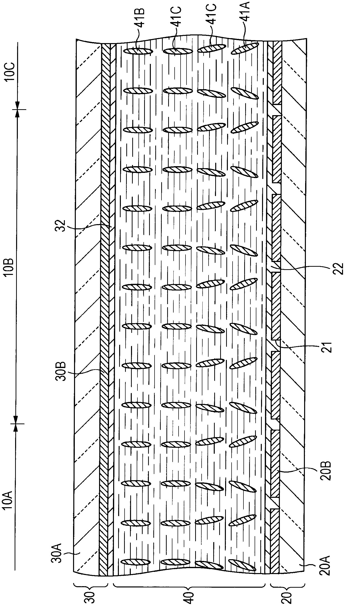
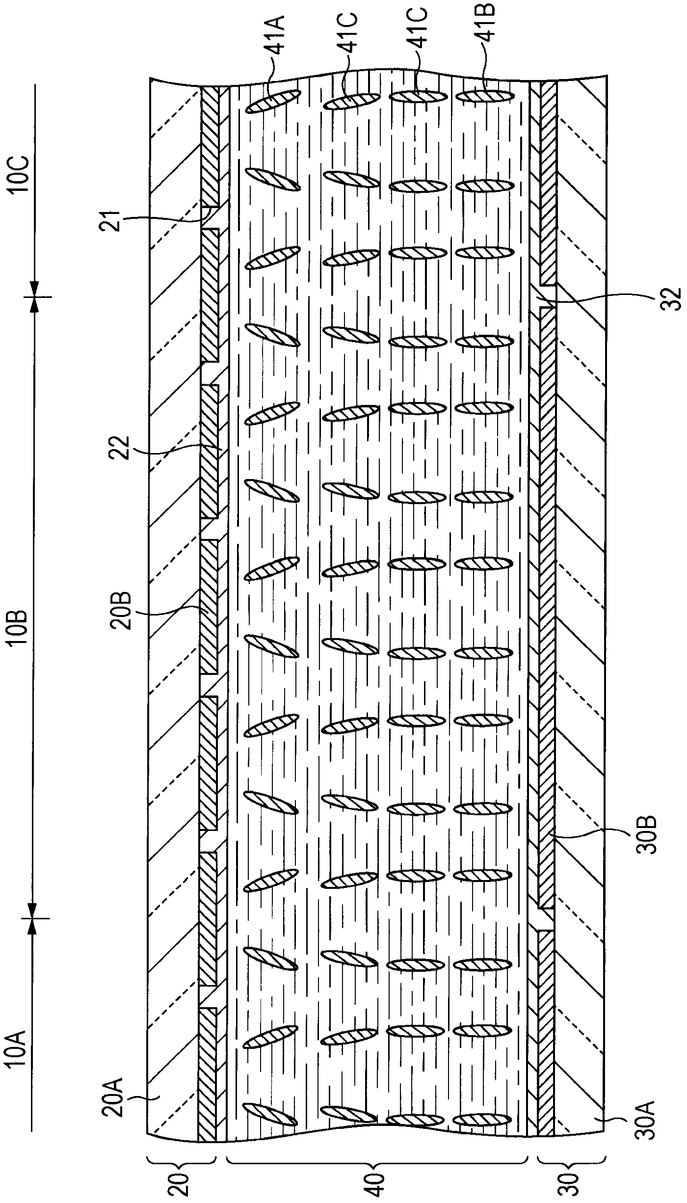
[0124] Embodiment 1 relates to the VA mode liquid crystal display device (or liquid crystal display element) according to the first embodiment of the present invention and relates to the liquid crystal display device (or liquid crystal display element) according to the first embodiment or the third embodiment of the present invention Production method. According to Embodiment 1, the first alignment film and the second alignment film (alignment films 22 and 32) are configured to contain one, two or more types of polymer compounds containing a crosslinked structure as a side chain (orientation treatment After the compound). In addition, the pretilt is imparted on the liquid crystal molecules by a cross-linked or polymerized compound. Here, before providing the liquid crystal layer 40, after forming the alignment films 22 and 32 containing one, two or more types of polymer compounds containing main chains and side chains (pre-alignment treatment compounds), While applying an ele...
Embodiment approach 2
[0253] Embodiment 2 relates to a liquid crystal display device according to the second embodiment of the present invention, and relates to methods of manufacturing liquid crystal display devices according to the second and third embodiments of the present invention.
[0254] In Embodiment 1, the post-alignment compound is obtained by crosslinking or polymerizing the crosslinkable functional group or polymerizable functional group in the pre-alignment compound containing a crosslinkable functional group or polymerizable functional group as a side chain. On the other hand, in Embodiment 2, the post-alignment compound is obtained by deforming the pre-alignment compound containing a photosensitive functional group as a side chain by irradiation with energy rays.
[0255] In Embodiment 2, the alignment films 22 and 32 are also configured to include one, two or more types of polymer compounds (compounds after the first alignment treatment) having a cross-linked structure in the side chain...
Embodiment 1
[0265] Example 1 relates to a liquid crystal display device (liquid crystal display element) and a manufacturing method thereof according to the first embodiment of the present invention, and a liquid crystal display device (liquid crystal display element) and a manufacturing method thereof according to the third embodiment of the present invention. In Example 1, later on Figure 15 The shown liquid crystal display device (liquid crystal display element) is manufactured through the following process.
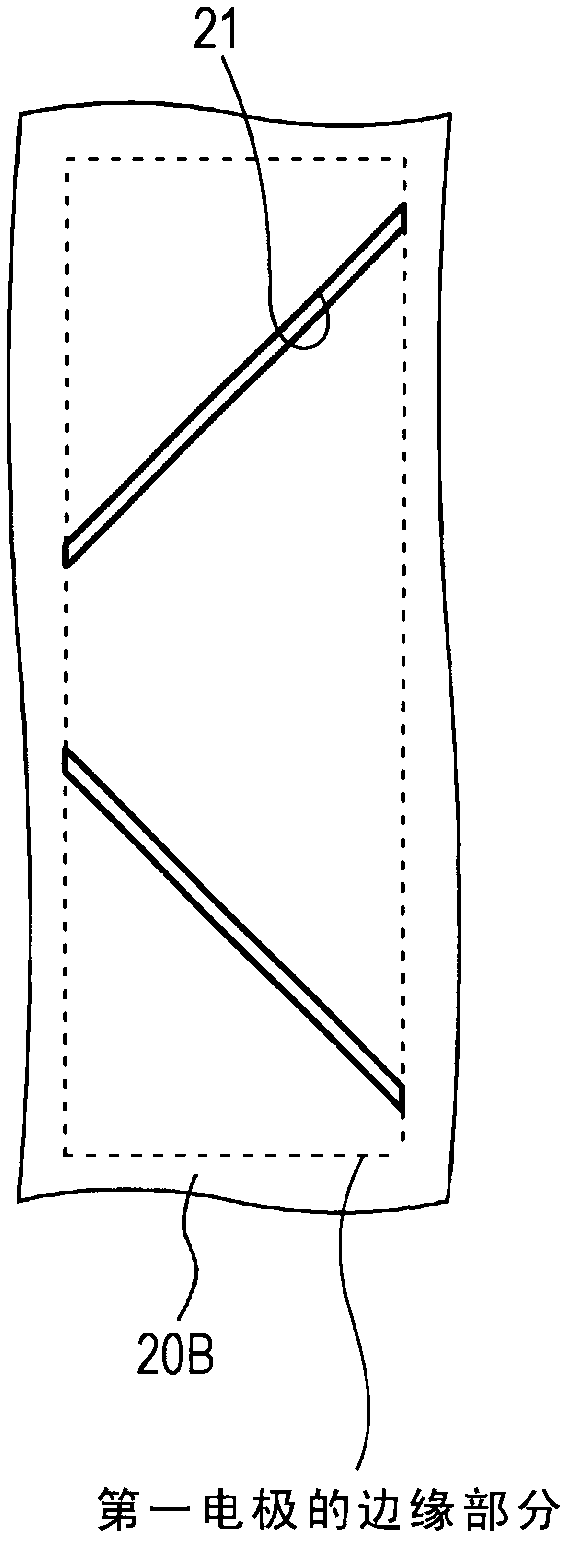
[0266] First, the TFT substrate 20 and the CF substrate 30 are prepared. A first electrode including a slit pattern (the width and pitch of the first slit portion 21 are 5 μm and 65 μm, respectively, and the first slit portion 21 is formed thereon is formed on one side of the glass substrate 20A having a thickness of 0.7 mm The width of each part of 20B is 60 μm, and the interval between the first electrode 20B and the other first electrode 20B is 5 μm) and the base material of the...
PUM
| Property | Measurement | Unit |
|---|---|---|
| Thickness | aaaaa | aaaaa |
| Thickness | aaaaa | aaaaa |
| Particle size | aaaaa | aaaaa |
Abstract
Description
Claims
Application Information