Array substrate, liquid crystal display panel and driving method

A liquid crystal display panel and array substrate technology, which is applied in the liquid crystal field, can solve the problems of light leakage at the via hole, irregular shape, and reduce the aperture ratio, so as to achieve the effect of uniform appearance, the same opening size, and avoiding horizontal stripes

Active Publication Date: 2015-04-15
BEIJING BOE OPTOELECTRONCIS TECH CO LTD
View PDF6 Cites 0 Cited by
  • Summary
  • Abstract
  • Description
  • Claims
  • Application Information

AI Technical Summary

Problems solved by technology

refer to figure 1 , whose gate lines 101 face the respective pixel units A (this area is surrounded by a gate line 101, two vertical data lines 102 and a common electrode line 103), which cannot effectively use the space, and at the same time, the source electrode is connected to the via hole B of the pixel electrode In the pixel unit display area A
At the same time, in order to prevent light leakage, it is often blocked by the black matrix BM (not shown in the figure) on the side of the color filter, but at the same time, the aperture ratio is greatly reduced, and because of the problem of box alignment accuracy, it often causes gaps at the via holes. light leak
[0004] In addition, in traditional ADS products with common electrode traces added, the BM on the line above the gate line blocks the thin film transistor TFT and traces, resulting in irregular shapes, which are inconsistent with the flat BM on the common electrode, so that in the final product there will be Horizontal stripes are formed, and the difference in brightness between adjacent rows causes abnormal display on the entire screen

Method used


Image

  • Array substrate, liquid crystal display panel and driving method
  • Array substrate, liquid crystal display panel and driving method
  • Array substrate, liquid crystal display panel and driving method

Examples


Embodiment Construction

[0021] Embodiments of the present invention provide an array substrate, a liquid crystal display panel and a driving method, which are used to increase the aperture ratio of a pixel unit, avoid horizontal stripes in display caused by different black matrices in adjacent rows, and improve display quality.

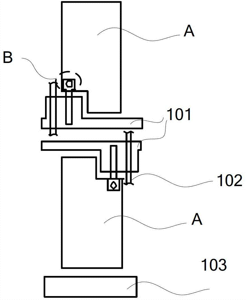
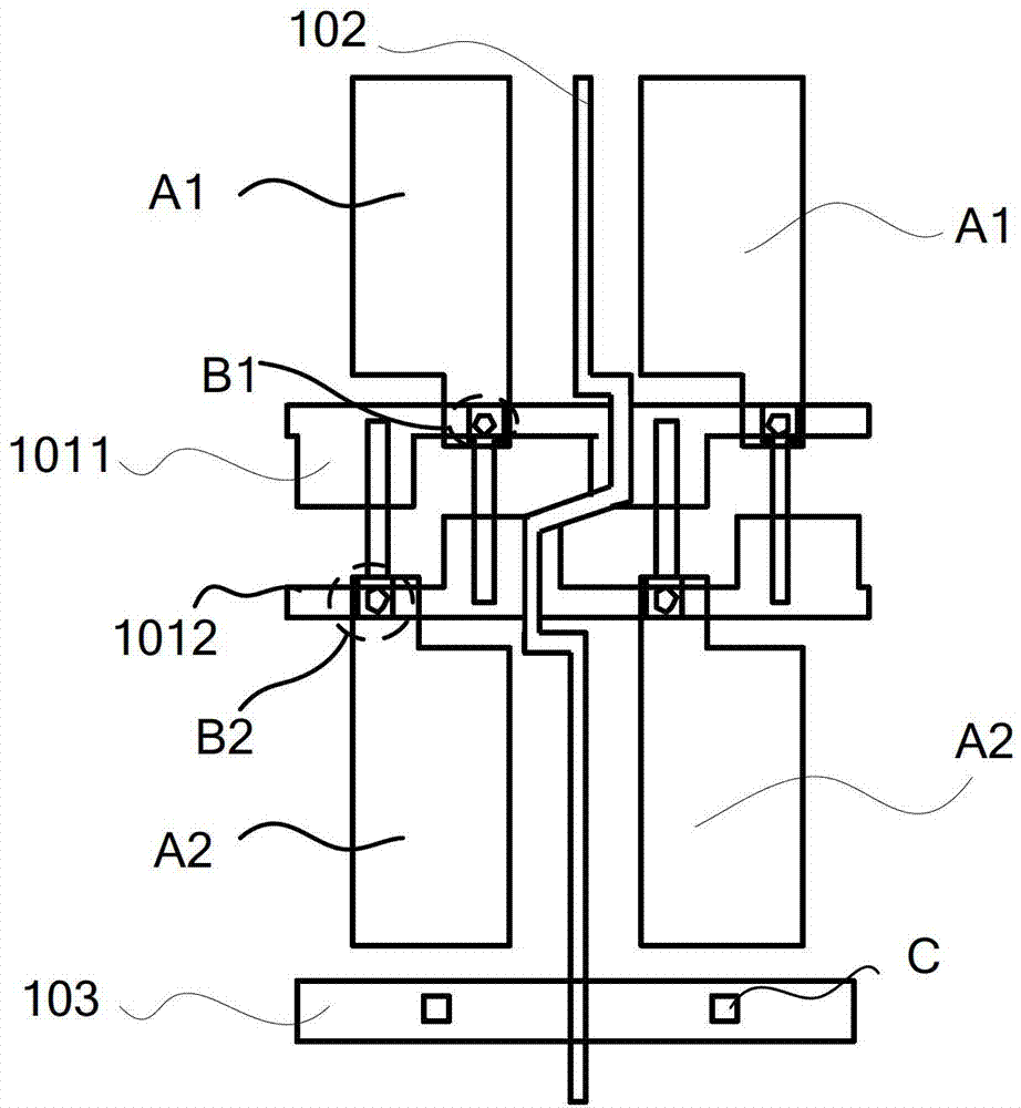
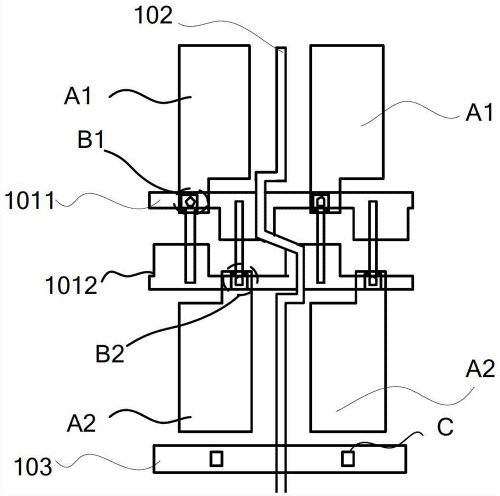
[0022] An array substrate provided by an embodiment of the present invention includes cross-arranged data lines and gate lines, and a pixel unit formed by surrounding the data lines and gate lines. The pixel unit includes a thin film transistor TFT and a pixel electrode. The TFT It includes a gate electrode, a source electrode and a drain electrode, the source electrode is connected to the data line, wherein two adjacent rows of gate lines are located between the driven adjacent two rows of pixel units, and the drain electrode is connected to the pixel unit The connection of the electrodes corresponds to between or on the gate lines of two adjacent rows driving the two adjace...


PUM


Abstract

An array substrate (100), a liquid crystal display panel and a driving method, which are used for increasing the aperture ratio of a pixel region, preventing display horizontal stripes caused by different shapes of black matrices of adjacent rows, and improving the display quality.The array substrate (100) includes a plurality of data lines (102) and a plurality of gate lines (101, 1011, 1012) in an intersecting arrangement, and a plurality of pixel units (A1, A2) in array arrangement enclosed by the plurality of data lines (102) and the plurality of gate lines (101). Each of the pixel units (A1, A2) includes a thin-film transistor (TFT) and a pixel electrode (104, 1041, 1042), the thin-film transistor (TFT) includes a gate electrode (G1, G2), a source electrode and a drain electrode (D1, D2), the source electrode is connected to the corresponding data line (102), the drain electrode (D1, D2) is connected to the pixel electrode (1041, 1042), two adjacent rows of gate lines (1011, 1012) are located between two adjacent rows of corresponding driven pixel units (A1, A2), and the connection position of the drain electrode (D1, D2) of each thin-film transistor (TFT) in the two adjacent rows of pixel units (A1, A2) and the pixel electrode (1041, 1042) is located between the two rows of gate lines (1011, 1012) or on the corresponding gate line (1011, 1012).

Description

technical field [0001] The invention relates to the field of liquid crystal technology, in particular to an array substrate, a liquid crystal display panel and a driving method. Background technique [0002] With the increasing demand for Advanced Super Dimension Switch (ADS) liquid crystal display products, the requirements for power consumption are also getting higher and higher, which requires the aperture ratio of the pixel unit to reach a higher level to reduce power consumption. In addition to process control, design improvement has become an important way to increase aperture ratio. [0003] In traditional ADS products that add common electrode traces, the common electrode traces are periodically connected to the ITO layer of the common electrode line through via holes, which acts as a parallel resistor to reduce resistance. refer to figure 1 , whose gate lines 101 face the respective pixel units A (this area is surrounded by a gate line 101, two vertical data line...

Claims


Application Information

Patent Timeline
Patent Type & Authority Patents(China)
IPC IPC(8): G02F1/1362G02F1/1368G02F1/133G09G3/36
CPCG09G2300/0465G02F1/133512G02F1/136286G02F1/136227G02F2201/40G02F1/134372G02F1/133G02F1/1368
Inventor 姜文博董学薛海林陈小川
Owner BEIJING BOE OPTOELECTRONCIS TECH CO LTD
Why Eureka
Try Eureka