PCB expansion compensation method
A technology of PCB board and compensation method, applied in electrical components, printed circuit parts, printed circuit manufacturing and other directions, can solve the problems of large expansion and shrinkage deviation of PCB board and low precision of PCB board.
- Summary
- Abstract
- Description
- Claims
- Application Information
AI Technical Summary
Problems solved by technology
Method used
Image
Examples
Embodiment Construction
[0020] Embodiments of the present invention are described in detail below in conjunction with accompanying drawings:
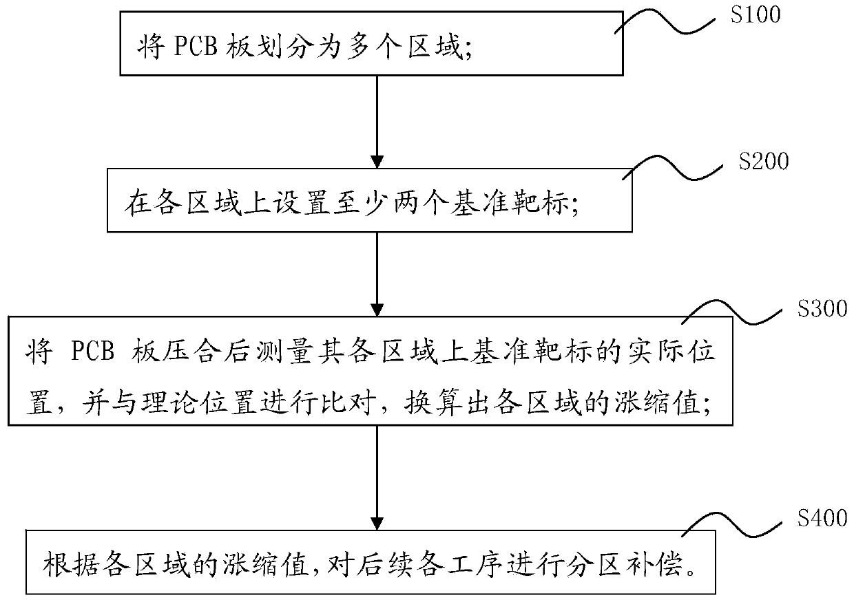
[0021] Such as figure 1 Shown, a kind of PCB expansion and contraction compensation method comprises the following steps:
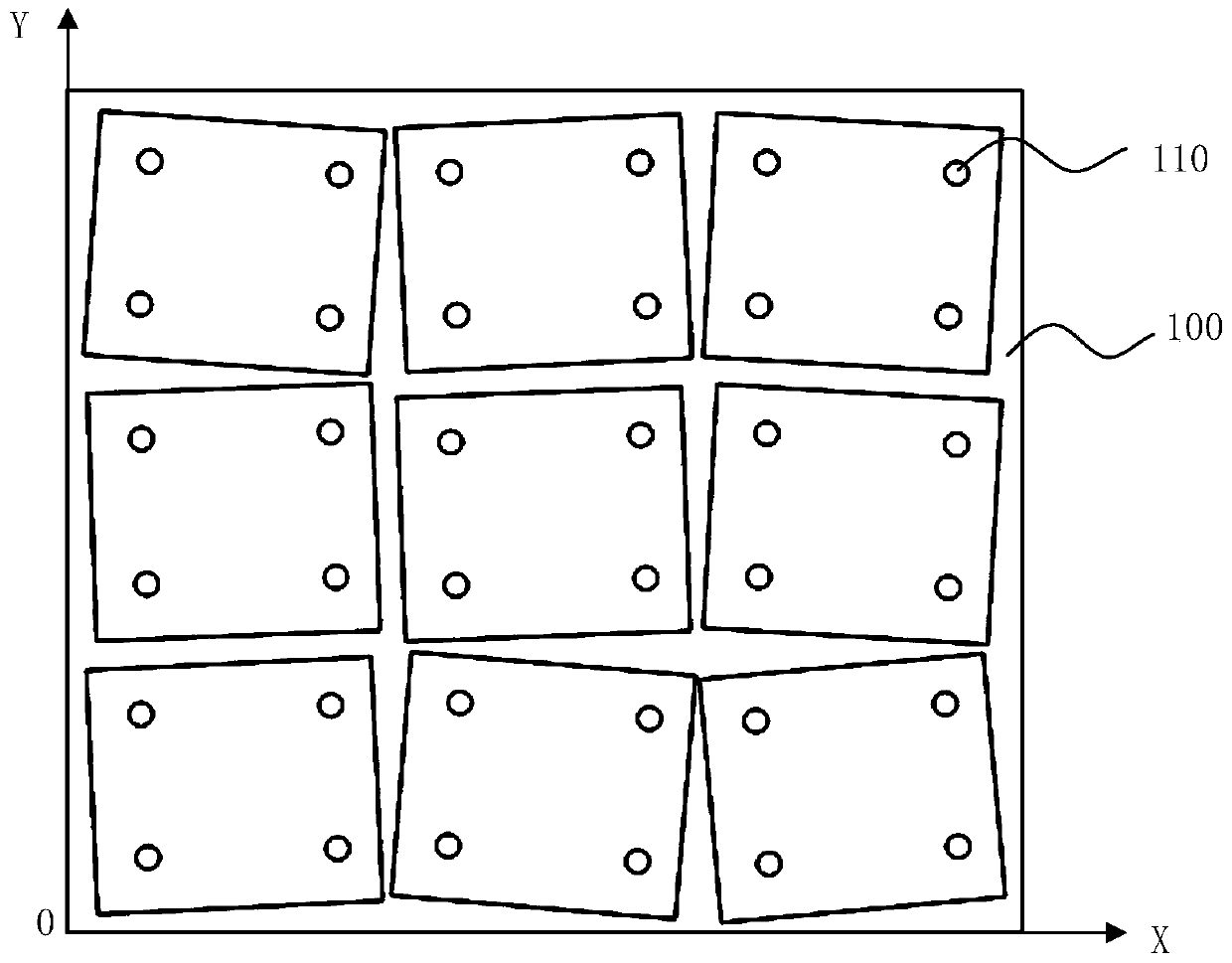
[0022] S100: Divide the PCB board into multiple areas;
[0023] S200: setting at least two reference targets on each area;
[0024] S300: Measure the actual position of the reference target on each area after pressing the PCB board, compare it with the theoretical position, and convert the expansion and contraction values of each area;
[0025] S400: According to the expansion and contraction values of each area, perform partition compensation for each subsequent process.
[0026] The above PCB board expansion and contraction compensation method divides the PCB board before lamination into multiple areas, and sets at least two reference targets on each area, measures the actual position of the reference target on each area of the...
PUM
 Abstract
Description
Claims
Application Information

