Method for manufacturing liquid-crystal display device
A technology of a liquid crystal display device and a manufacturing method, which can be applied to optics, instruments, nonlinear optics, etc., and can solve problems such as the reduction of white display transmittance
- Summary
- Abstract
- Description
- Claims
- Application Information
AI Technical Summary
Problems solved by technology
Method used
Image

Examples
Embodiment approach 1
[0131]A method of manufacturing the liquid crystal display device of Embodiment 1 will be described below. The liquid crystal display device manufactured by the method for manufacturing a liquid crystal display device according to Embodiment 1 can be suitably used for TV panels, digital signage, medical monitors, electronic books, monitors for PCs, panels for tablet terminals, and mobile phone terminals. panel etc.
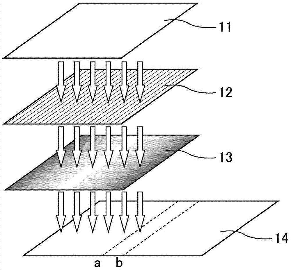
[0132] Before performing the photo-alignment treatment, first, a pair of substrates including a TFT substrate and a counter substrate sandwiching a liquid crystal layer are prepared. Figure 14 is a schematic plan view of the TFT substrate in Embodiment 1, Figure 15 is a schematic plan view of a counter substrate in Embodiment 1. FIG.
[0133] Such as Figure 14 As shown, as the TFT substrate, for example, a substrate in which scanning signal lines 21 , data signal lines 22 , TFT 23 , and pixel electrodes 24 are arranged on a glass substrate via an insulating ...
Embodiment approach 2
[0158] The manufacturing method of Embodiment 2 differs from Embodiment 1 in that the shape of the light-transmitting portion of the photomask used is different, but is the same as Embodiment 1 except that.
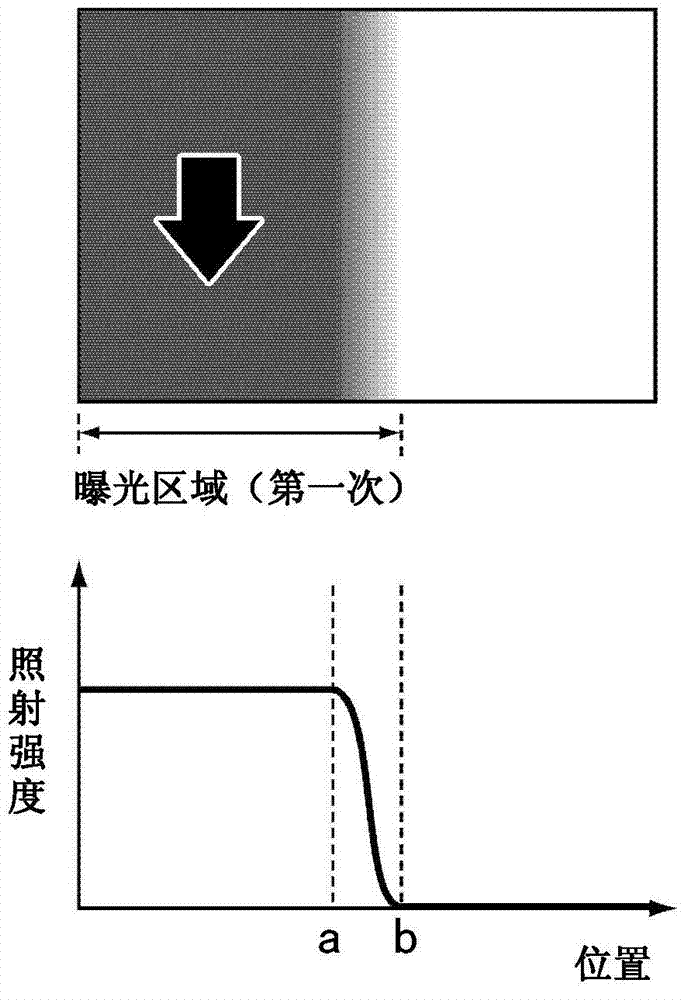
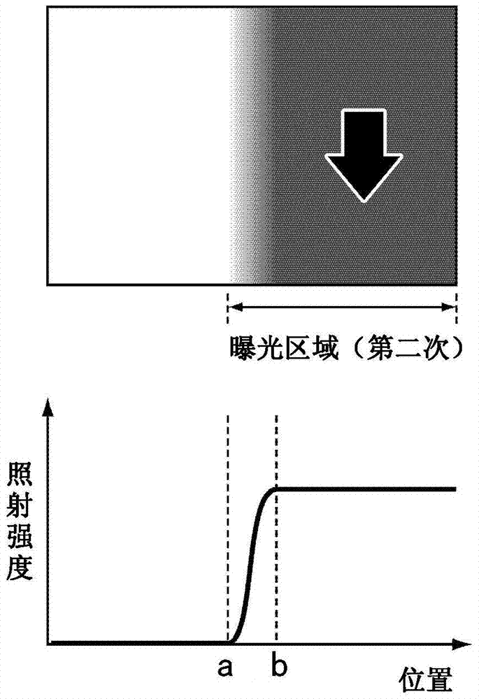
[0159] Figure 26 is a schematic plan view of a photomask (illuminance adjustment plate) used in Embodiment 2. The shapes of the sub-regions 74a, 74b constituting both ends of the light-transmitting portions 71a, 71b of the photomasks 70a, 70b will be described in detail. The outer edges of the sub-regions 74a, 74b are defined by a first straight line and a second straight line extending from both ends of the boundary line between the main regions 73a, 73b and the sub-regions 74a, 74b to the opposite side of the main regions 73a, 73b. two straight lines. The first straight line is parallel to the straight line constituting the outer edge of the main regions 73a, 73b, and the second straight line is in an oblique direction relative to the straight line constituting the o...
Embodiment approach 3
[0163] The manufacturing method of Embodiment 3 is the same as Embodiment 1 except that the shape of the light-transmitting portion of the photomask used is different from Embodiment 1.
[0164] Figure 30 is a schematic plan view of a photomask (illuminance adjustment plate) used in Embodiment 3. FIG. The shapes of the sub-regions 74a, 74b constituting both ends of the light-transmitting portions 71a, 71b of the photomasks 70a, 70b will be described in detail. The outer edges of the sub-regions 74a, 74b are composed of first curved lines and second curved lines extending from the two ends of the boundary line between the main regions 73a, 73b and the sub-regions 74a, 74b to the side opposite to the main regions 73a, 73b. curve composition. The rate of change of the first curve and the second curve follows a sinusoidal function. The first curve and the second curve intersect on a line bisecting the main areas 73a, 73b up and down. That is, the outer edges of the sub-region...
PUM
| Property | Measurement | Unit |
|---|---|---|
| thickness | aaaaa | aaaaa |
| wavelength | aaaaa | aaaaa |
Abstract
Description
Claims
Application Information
 - R&D Engineer
- R&D Manager
- IP Professional
- Industry Leading Data Capabilities
- Powerful AI technology
- Patent DNA Extraction
Browse by: Latest US Patents, China's latest patents, Technical Efficacy Thesaurus, Application Domain, Technology Topic.
© 2024 PatSnap. All rights reserved.Legal|Privacy policy|Modern Slavery Act Transparency Statement|Sitemap