
A method for allocating addresses of solid-state storage devices

A technology of solid-state storage device and allocation method, applied in the direction of memory address/allocation/relocation, etc., can solve the problems of ineffective reduction of read and write request conflicts, performance degradation of solid-state storage devices, and increase of read request response time, etc. Prioritization, conflict avoidance, effect of reducing response time

Active Publication Date: 2017-01-11
HUAZHONG UNIV OF SCI & TECH
View PDF4 Cites 0 Cited by
  • Summary
  • Abstract
  • Description
  • Claims
  • Application Information

AI Technical Summary

Problems solved by technology

In particular, the location of the data accessed by the read request has been determined according to the address. When the write request occupies channel resources, the response time of the read request continues to rise, and the performance of the solid-state storage device decreases significantly.
[0014] Dynamic address allocation can improve the write performance of solid-state storage devices, but it cannot effectively reduce conflicts between read and write requests, and the read performance is lower than static address allocation.

Method used

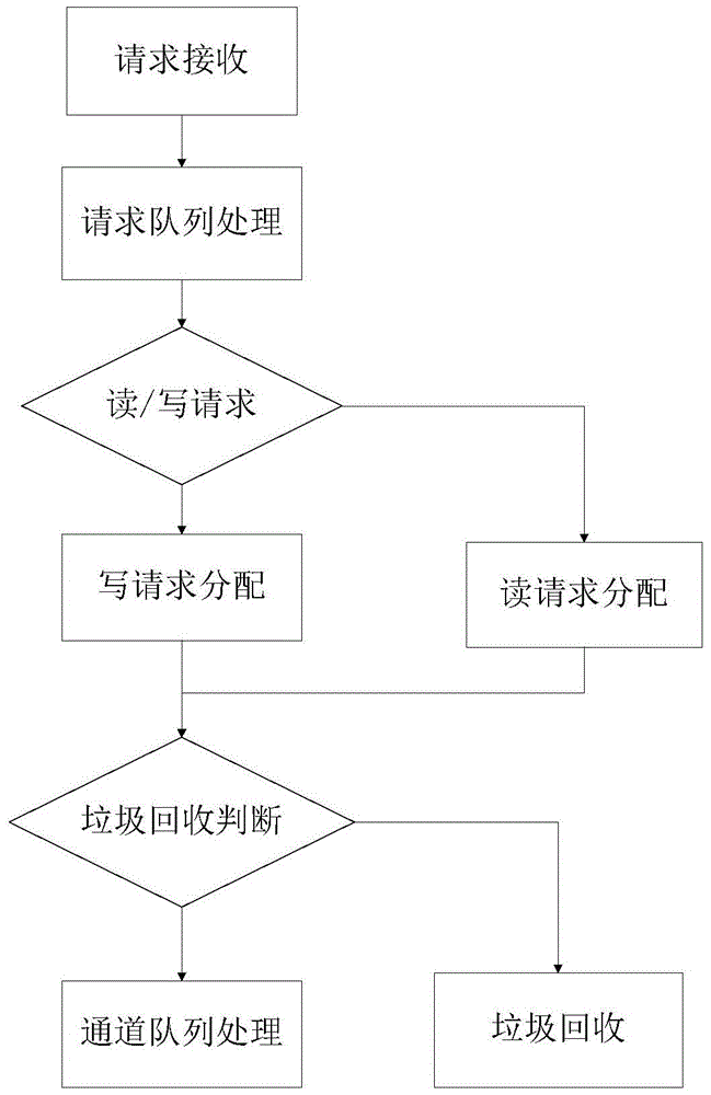
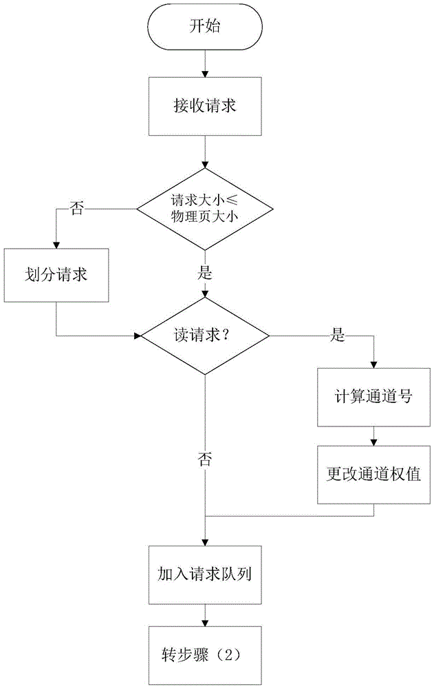
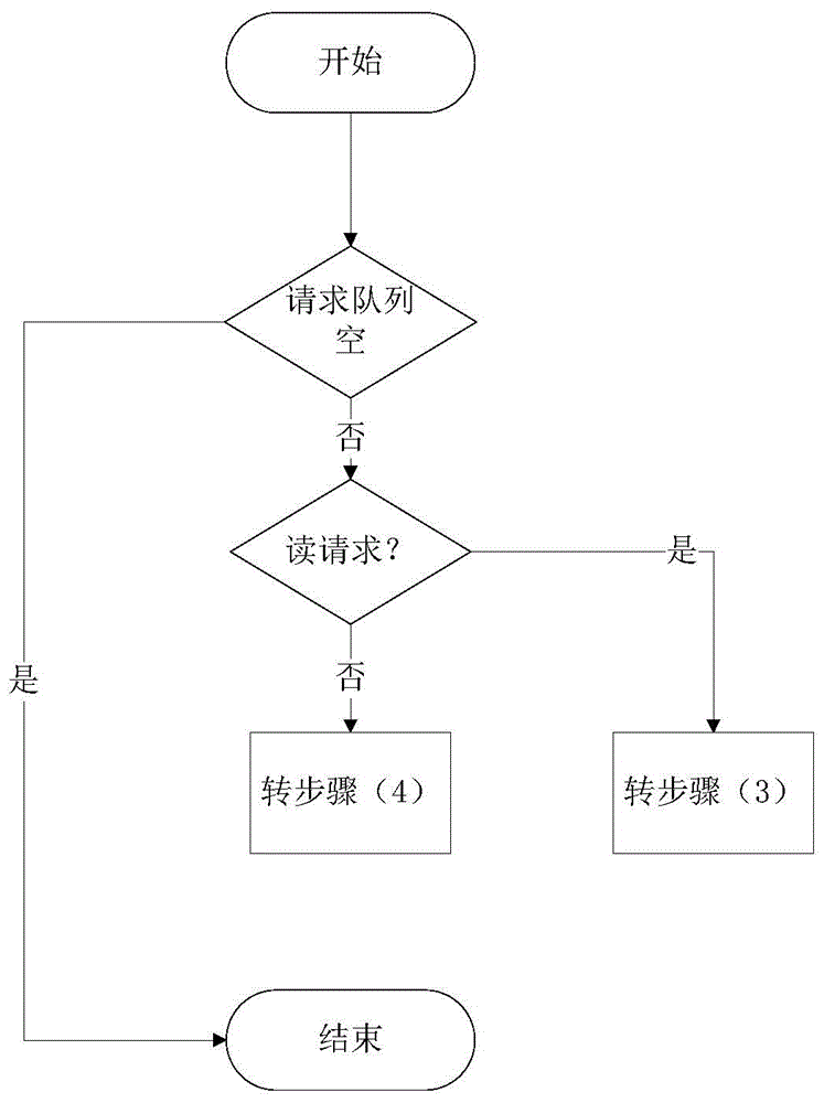

Image

  • A method for allocating addresses of solid-state storage devices
  • A method for allocating addresses of solid-state storage devices
  • A method for allocating addresses of solid-state storage devices

Examples


Embodiment Construction

[0064] In order to make the object, technical solution and advantages of the present invention clearer, the present invention will be further described in detail below in conjunction with the accompanying drawings and embodiments. It should be understood that the specific embodiments described here are only used to explain the present invention, not to limit the present invention. In addition, the technical features involved in the various embodiments of the present invention described below can be combined with each other as long as they do not constitute a conflict with each other.

[0065] In order to understand the present invention clearly, relevant concepts are explained below:

[0066] NAND flash memory chip: The flash memory chip technology was invented by Toshiba in 1984. It is an electronic erasable programmable read-only memory. It is characterized by a simple structure and a considerable amount of data storage in a semiconductor per unit area. The side effect of t...


PUM


Abstract

The invention discloses an address distribution method of a solid-state storage device, belongs to the field of solid-stage storage, and aims at solving the problem of conflict of read and write requests in the existing distribution strategy and the problem that the request response time is prolonged under the read and write request mixed workload. The address distribution method is applicable to a multi-channel solid-stage storage device based on flash memory. The method comprises the steps of distributing weights of a channel, distributing physical addresses, and building a conflict prediction and avoiding mechanism. According to the address distribution method of the solid-stage storage device, different weights are distributed to read and write requests and garbage recovery operation; the weights can be adjusted according to user requirements in order to adapt to different read and write performance requirements, and the parallelism in the solid-stage storage device can be fully utilized; a proper physical address is selected for the write request according to the load condition, thus the conflict between write and read can be decreased, and the block of the garbage recovery operation to the write request is reduced; the read and write response time of the solid-state storage device is decreased, and the performances of the solid-stage storage device are improved.

Description

technical field [0001] The invention belongs to the technical field of solid-state storage, and more particularly relates to an address allocation method of a solid-state storage device. Background technique [0002] Solid-state storage devices are a new type of computer storage devices that are different from mechanical hard disks. Compared with traditional hard disks, flash-based solid-state storage devices have the characteristics of high density, low energy consumption, no noise, anti-vibration, etc., and it has lower read and write delays and higher throughput rates. [0003] Due to the characteristics of flash media, flash-based solid-state storage devices also have the following drawbacks: [0004] (1) Erase first and then write: the flash memory medium cannot be updated in situ when writing data, and the physical block of the target address needs to be erased first, and then the data is updated. The basic units of the erase operation and the read and write operatio...

Claims


Application Information

Patent Timeline
Patent Type & Authority Patents(China)
IPC IPC(8): G06F12/02
Inventor 童薇罗锐刘景宁冯丹余晨晔冒伟
Owner HUAZHONG UNIV OF SCI & TECH
Learn More