A composite packaging product with self-powered electronic display elements
A technology of electronic display components and composite packaging, applied in packaging, wrapping paper, transportation and packaging, etc., can solve the problems of electronic devices not working, environmental pollution, battery costs, etc., to achieve easy operation and quality control, high sensitivity, The effect of high power generation
- Summary
- Abstract
- Description
- Claims
- Application Information
AI Technical Summary
Problems solved by technology
Method used
Image
Examples
Embodiment 1
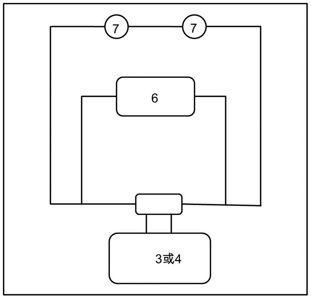
[0032] see Figure 1a , 1b and Figure 3a , the composite packaging product includes a lower layered structure 1 and an upper layered structure 2, and the upper and lower layered structures 1, 2 can be properly preprocessed before being adhered to each other.
[0033]Specifically, the lower layered structure 1 includes a surface layer 12, a first bonding layer 13 and a protective layer 14 that are superimposed on each other. The surface layer 12 is welded with an electronic display element 11, and the first bonding layer 13 is used for The lower side of the layer 12 is bonded to the upper side of the protective layer 14, and the first adhesive layer 13 remains on the surface layer 12 after the surface layer 12 is torn relative to the protective layer 14; the upper layer structure 2 includes The pattern layer 21 and the second adhesive layer 22 superimposed on each other, the pattern layer 21 and the second adhesive layer 22 are hollowed out according to the position of the el...
Embodiment 2
[0038] see Figure 1a , 1b and Figure 3b , the composite packaging is formed by aligning and adhering the lower layered structure 1 and the upper layered structure 2, and the upper and lower layered structures can be properly preprocessed before being adhered to each other.
[0039] Specifically, the lower layered structure 1 includes a surface layer 12, a first bonding layer 13 and a protective layer 14 that are superimposed on each other. The surface layer 12 is welded with an electronic display element 11, and the first bonding layer 13 is used for The lower side of the layer 12 is bonded to the upper side of the protective layer 14, and the first adhesive layer 13 remains on the surface layer 12 after the surface layer 12 is torn relative to the protective layer 14; the upper layer structure 2 includes The pattern layer 21 and the second adhesive layer 22 superimposed on each other, the pattern layer 21 and the second adhesive layer 22 are hollowed out according to the p...
PUM
 Abstract
Description
Claims
Application Information


