
Method of testing semiconductor device and apparatus of testing semiconductor device

An inspection method and inspection device technology, applied in the field of inspection of semiconductor devices and inspection devices of semiconductor devices, to achieve the effect of accurate good or bad judgment

Inactive Publication Date: 2015-03-25
KK TOSHIBA
View PDF5 Cites 0 Cited by
  • Summary
  • Abstract
  • Description
  • Claims
  • Application Information

AI Technical Summary

Problems solved by technology

In other words, in the inspection using a thermal resistance, the resistance changes less and errors are likely to occur

Method used


Image

  • Method of testing semiconductor device and apparatus of testing semiconductor device
  • Method of testing semiconductor device and apparatus of testing semiconductor device
  • Method of testing semiconductor device and apparatus of testing semiconductor device

Examples


no. 1 approach )

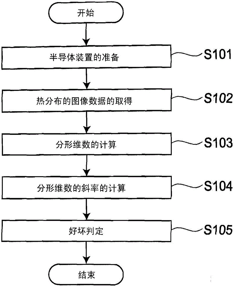
[0020] figure 1 It is a flowchart illustrating the inspection method of the semiconductor device according to the first embodiment.

[0021] Such as figure 1 As shown, this embodiment has the following steps: preparation of semiconductor device (step S101), acquisition of image data of thermal distribution (step S102), calculation of fractal dimension (step S103), calculation of slope of fractal dimension (step S104), and good or bad judgment (step S105).

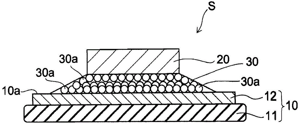
[0022] In the preparation of the semiconductor device shown in step S101 , a semiconductor device in which a semiconductor element and a substrate are bonded by a bonding material containing metal fine particles is prepared. A semiconductor device is an object to be judged whether the junction is good or bad.

[0023] In acquiring the image data of the heat distribution shown in step S102 , the semiconductor device prepared in step S101 is heated, and the image data of the heat distribution in the semiconductor device is...

no. 2 approach )

[0080] Next, an inspection device for a semiconductor device according to a second embodiment will be described.

[0081] Figure 9 It is a figure which exemplifies the inspection apparatus of the semiconductor device of 2nd Embodiment.

[0082] Such as Figure 9 As shown, the semiconductor device inspection device 210 of this embodiment includes a heating unit 201 , an image acquisition unit 202 , and a determination unit 203 . The inspection device 210 is a device that implements the semiconductor device inspection method of the first embodiment described above.

[0083] The heating unit 201 has a heat source for heating the semiconductor device S (for example, a high-frequency oscillator, a lamp). It is desirable that the heat source has a structure capable of intensively heating the semiconductor device S. For example, it is desirable that the range of the heat source is approximately equal to the size of the semiconductor device S. FIG. By intensively heating the sem...


PUM


Abstract

According to one embodiment, in a method of testing a semiconductor device, the semiconductor device has a semiconductor element and a substrate which are bonded by bonding material including metal fine particles. Image data of a heat distribution in the semiconductor device are temporally acquired while heating the semiconductor device. A time change of a fractal dimension based on the image data is calculated. An inclination of the time change of the fractal dimension is calculated. The inclination and a reference inclination set in advance are compared. Whether or not the semiconductor device is good is determined.

Description

[0001] (References to related applications) [0002] This application is based on the benefit of the rights of the prior Japanese Patent Application No. 2013-191108 for which it applied on September 13, 2013, claims the benefit, and takes in the whole content here by reference. technical field [0003] The embodiments described here generally relate to a semiconductor device inspection method and a semiconductor device inspection device. Background technique [0004] A bonding material is used for the junction between the semiconductor element and the substrate. For the bonding material, materials such as Sn-95Pb to Sn-90Pb and SnAg are used. In addition, in recent years, there have been diffusion bonding, sinter bonding using metal fine particles such as Ag, Au, and Cu, and the like. The quality judgment of these junctions is judged by observing junctions of semiconductor elements one by one using a magnifying glass or the like. In addition, the joint thickness of the si...

Claims


Application Information

Patent Timeline
Patent Type & Authority Applications(China)
IPC IPC(8): G01N25/00
CPCG01R31/311G01N25/72
Inventor 久里裕二小谷和也佐佐木遥平塚大祐松村仁嗣北泽秀明安达健二
Owner KK TOSHIBA
Learn More