
Board inspection apparatus

A substrate inspection and substrate technology, which is applied to measurement devices, optical devices, televisions, etc., can solve problems such as leakage and reduce inspection accuracy, and achieve the effect of realizing high speed, improving inspection accuracy, and realizing inspection accuracy.

Active Publication Date: 2017-09-29
CKD
View PDF12 Cites 13 Cited by
  • Summary
  • Abstract
  • Description
  • Claims
  • Application Information

AI Technical Summary

Problems solved by technology

[0006] However, in a board inspection device that simultaneously inspects both the front and back sides, part of the light irradiated to one side of the printed board may pass through the hole formed in the printed board or the glass epoxy resin constituting the base board, and leak. to the other side of the printed substrate
As a result, when inspecting the other side of the printed circuit board, it may be affected by the light leaked from one side, thereby reducing the inspection accuracy.

Method used


Image

  • Board inspection apparatus
  • Board inspection apparatus
  • Board inspection apparatus

Examples


Embodiment Construction

[0070] Hereinafter, one embodiment will be described with reference to the drawings. First, the configuration of a printed circuit board to be inspected will be described in detail. In the present embodiment, a two-layer substrate (double-sided substrate) on which electronic components are mounted on both the front and rear surfaces is used as an inspection object.

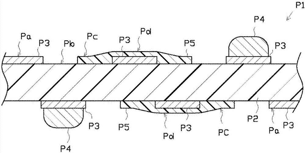
[0071] Such as figure 2 As shown, the printed board P1 has a flat plate shape, and electrode patterns P3 made of copper foil are provided on both front and back surfaces of a base board P2 made of glass epoxy resin or the like. Furthermore, the solder paste P4 which is a measurement object is printed and formed in the predetermined position (bonding land or pad, etc.) of the electrode pattern P3. The region where this solder paste P4 is printed is called "solder printing region". The parts other than the solder printing area are collectively referred to as "background area". The area of ​​the etching film P5 ...


PUM


Abstract

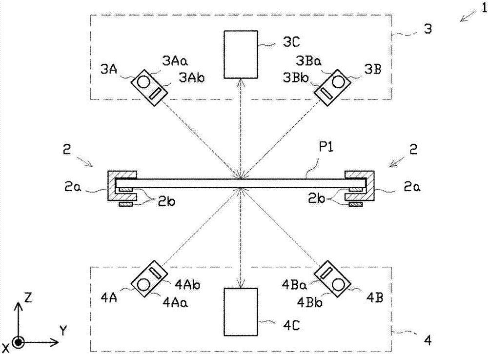
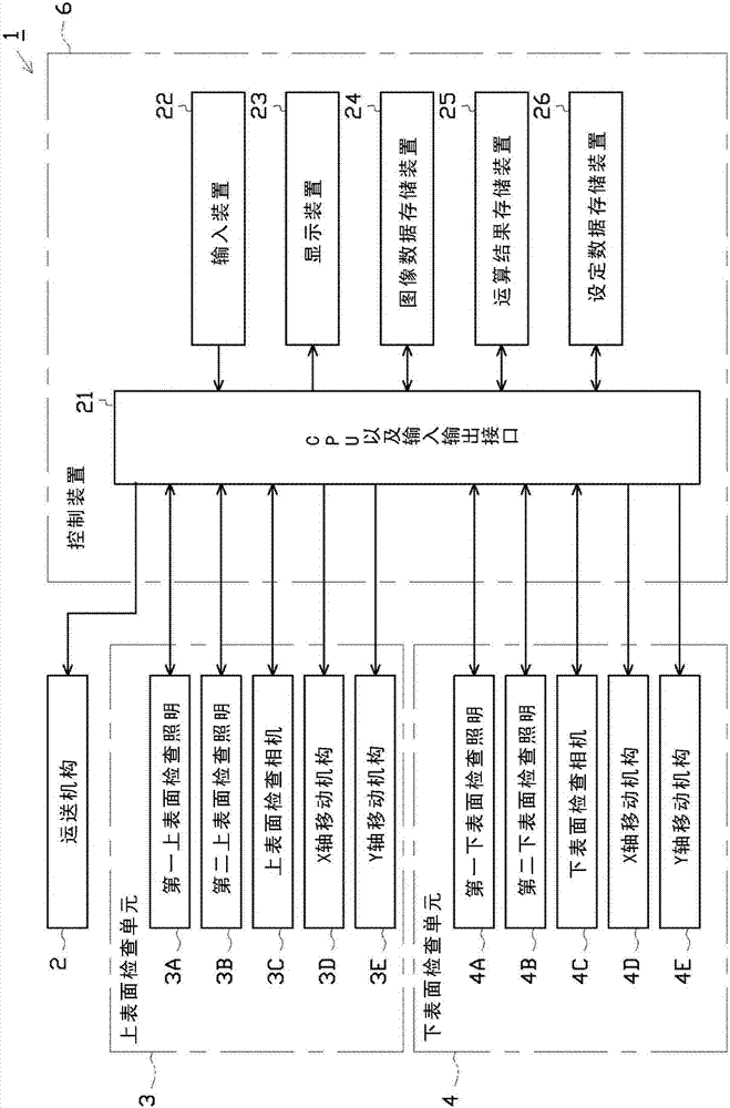
The invention provides a board inspection apparatus which can realize inspection precision increase related in two-face inspection of a board and furthermore can realize high speed in inspection. The board inspection apparatus (1) comprises an upper face inspection unit (3) configured to perform an inspection with regard to an the upper face (surface) side of the printed circuit board (P1), a lower face inspection unit (4) configured to perform an inspection with regard to a lower face (rear face) side of the printed circuit board (P1). The inspection unit (3,4) are provided with inspection illumination devices (3A,4A) which irradiate a strip pattern to the printed circuit board (P1), and inspection cameras (3C,4C) which perform photographing on the printed circuit board (P1). Furthermore, a specific process is carried out to alternately perform one imaging process among a plurality of imaging processes with regard to the predetermined inspection area by the upper face inspection unit (3) and one imaging process among a plurality of imaging processes with regard to the predetermined inspection area by the lower face inspection unit (4).

Description

technical field [0001] The present invention relates to a board inspection device for inspecting both front and back sides of a printed board or the like. Background technique [0002] Generally, in a printed circuit board on which electronic components are mounted on both the front and back surfaces, electrode patterns are provided on both the front and back surfaces of a base substrate made of glass epoxy resin, and these are protected by a resist film. [0003] In the production line for mounting electronic components on the above-mentioned printed circuit board, first, solder paste is printed on predetermined positions on both the front and rear surfaces of the printed circuit board (solder printing process). Next, an adhesive is applied to predetermined positions on both the front and rear surfaces of the printed circuit board (adhesive application step). Then, electronic components are mounted on both the front and rear surfaces of the printed circuit board (mounting ...

Claims


Application Information

Patent Timeline
Patent Type & Authority Applications(China)
IPC IPC(8): G01N21/956G01N21/01G01B11/25
CPCG01B11/25G01N21/01G01N21/956G01N2021/0162G01N2021/95638G01N21/9501G01N2021/95646G01N2201/12H04N23/56H04N23/90
Inventor 梅村信行加藤章大山刚坂井田宪彦
Owner CKD
Learn More