Preparation method of TEM analysis sample

A sample and extension direction technology, applied in the preparation of test samples, semiconductor/solid-state device manufacturing, electrical components, etc., can solve the problem of incomplete acquisition of bridging defect morphology and position, integrated circuit short circuit, and difficulty in judging bridging defects The specific reasons for the formation and other issues

Active Publication Date: 2015-04-29
SEMICON MFG INT (SHANGHAI) CORP
View PDF8 Cites 6 Cited by
  • Summary
  • Abstract
  • Description
  • Claims
  • Application Information

AI Technical Summary

Problems solved by technology

When manufacturing the above-mentioned on-wafer structure, due to the influence of structure, process and other factors, there may be bridging defects 4 between the contact holes, which is due to the diffusion barrier layer 2 and the metal line 3 during the preparation process The deposited diffusion barrier layer 2 and metal line 3 materials remain between the contact holes, and these remaining materials form bridging defects 4, which will lead to short circuits when the components in the integrated circuit are working
However, the TEM samples obtained by X-Cut can only obtain the image of the bridging in the X direction, so that the morphology and position of the bridging defects cannot be completely obtained, and it is difficult to determine the specific reasons for the formation of the bridging defects. Therefore, it is necessary to follow the The direction perpendicular to the bridging defect ( figure 1 in the Y direction) to cut in order to obtain the Y direction image of the bridging defect
However, if the conventional sample preparation method is adopted, in the Y-Cut sample formed by cutting, the metal wire with a certain thickness is included in the contact hole structure, and the image obtained by the metal wire with a certain thickness in the TEM analysis is relatively dark, so it will be There is occlusion of the bridging defect image, so the image of the bridging defect cannot be seen from the obtained Y-Cut sample image

Method used


Image

  • Preparation method of TEM analysis sample
  • Preparation method of TEM analysis sample
  • Preparation method of TEM analysis sample

Examples


preparation example Construction

[0024] Such as Figure 4 As shown, the invention provides a kind of preparation method of TEM analysis sample, comprising:

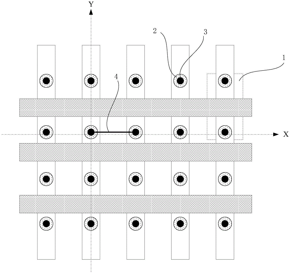
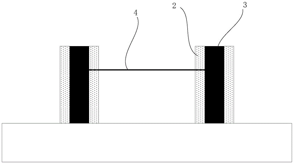
[0025] providing a wafer to be inspected, the wafer is provided with a first contact hole structure and a second contact hole structure, and a bridging defect is formed between the first contact hole structure and the second contact hole structure;

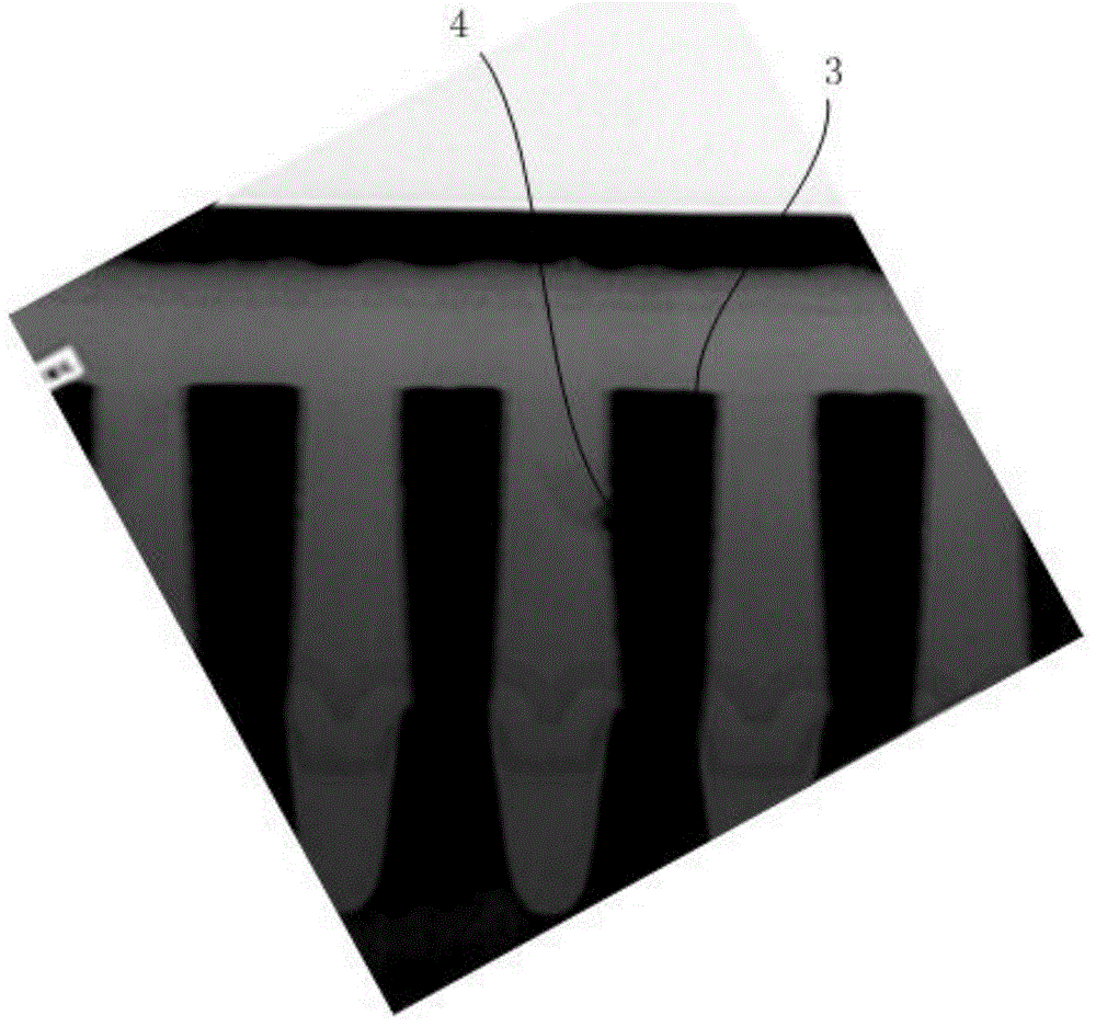
[0026] cutting the first contact hole structure along a direction perpendicular to the extending direction of the bridging defect to obtain a first sample including a first cutting surface, the first cutting surface exposing the metal line of the first contact hole structure;

[0027] removing the metal lines of the first contact hole structure in the first cutting plane;

[0028] The first sample is cut along the direction perpendicular to the extending direction of the bridging defect to remove the second contact hole structure, and a sample for TEM analysis is obtained.


PUM


Abstract

The invention provides a preparation method of a TEM analysis sample. A metal wire in a contact hole structure which is in bridge connection with one side with defects and a contact hole structure on the other side are removed in a process of forming a sample, so that the problem that a bridge connection defect image is shielded by a relatively dark metal wire image when bridge connection defects are observed in the Y direction is avoided.

Description

technical field [0001] The invention relates to the technical field of semiconductors, in particular to a method for preparing a sample for TEM (Transmission electron microscope, transmission electron microscope) analysis. Background technique [0002] In the semiconductor manufacturing process, it is often necessary to analyze the structure and material of the device. Commonly used means include using a scanning electron microscope (Scanning Electron Microscope, SEM) and a transmission electron microscope (Transmission electron microscope, TEM) to observe and analyze the microscopic state of the sample to be analyzed. [0003] The working principle of TEM is to project an accelerated and concentrated electron beam onto a very thin sample, and the electrons collide with atoms in the sample to change their direction, thereby producing solid angle scattering. The size of the scattering angle is related to the density and thickness of the sample, so images with different light...

Claims


Application Information

Patent Timeline
Patent Type & Authority Applications(China)
IPC IPC(8): G01N1/28H01L21/768
Inventor 殷原梓李日鑫高保林赵利利张菲菲
Owner SEMICON MFG INT (SHANGHAI) CORP
Why Eureka
Try Eureka