Overcoming multiple reflections in packages and connectors at high speed broadband signal routing

A broadband signal and connector technology, applied in the field of semiconductor packaging systems, can solve the problems of signal quality degradation, nonlinear signal insertion loss deviation, etc.

Inactive Publication Date: 2015-05-06
MARVELL ASIA PTE LTD
View PDF8 Cites 10 Cited by
  • Summary
  • Abstract
  • Description
  • Claims
  • Application Information

AI Technical Summary

Problems solved by technology

Multiple discontinuities cause undesired reflections in the wideband signal being carried in the trace
The nonlinear signal distortion due to this multiple discontinuity is known as "insertion loss skew", which degrades the quality of the signal propagating through the transmission line

Method used


Image

  • Overcoming multiple reflections in packages and connectors at high speed broadband signal routing
  • Overcoming multiple reflections in packages and connectors at high speed broadband signal routing
  • Overcoming multiple reflections in packages and connectors at high speed broadband signal routing

Examples


Embodiment Construction

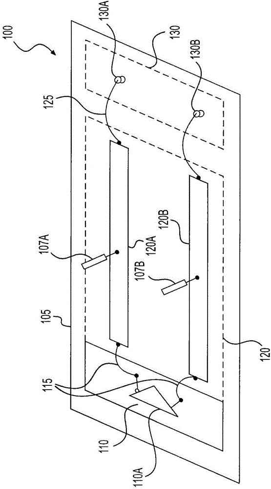
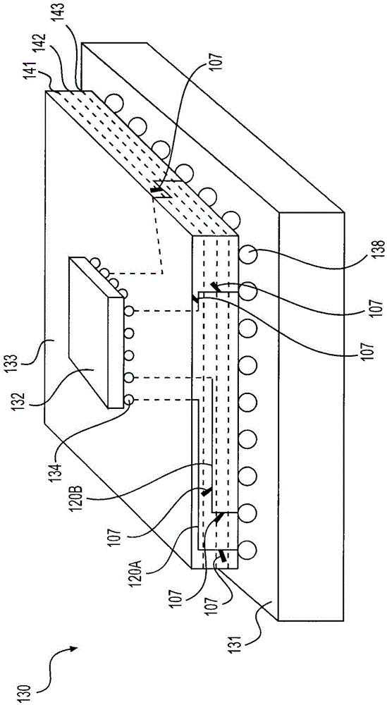
[0016] Figure 1A An example of a semiconductor IC package 100 is shown that includes a package body 105 having a semiconductor chip 110 having an input-output (I / O) unit 110A. The package body 105 further includes a transmission line 120 comprising a pair of transmission lines (traces) 120A and 120B coupled to the input-output (I / O) unit 110A via a first coupler 115, wherein the pair of transmission lines 120A and 120B are configured For transmitting differential signals. Second coupler 125 couples transmission lines 120A and 120B to respective ones of terminals 130A and 130B of terminals 130 . As shown, transmission lines 120A and 120B also include stubs 107A and 107B, respectively.

[0017] In operation, I / O unit 110A generates or receives high-speed digital or analog I / O signals. For example, I / O unit 110A generates or receives signals having a line rate of 25.78125 Gbps, or a data signaling rate compliant with the 25 Gbps 802.3bj standard. I / O unit 110A includes circu...


PUM


Abstract

Discussed herein is a semiconductor package and a method of overcoming multiple reflections while transmitting high speed broadband signals through the semiconductor package. The semiconductor package includes at least one trace having a first terminal that is configured to receive a broadband signal and a second terminal configured to output the broadband signal. The semiconductor package includes a stub which is positioned along a longitudinal length of the trace and is configured to reduce broadband reflections in the trace by causing multi-frequency reflections to destructively interfere with at least some broadband reflections in the trace that occur due to impedance discontinuities. The stub parameters such as stub length, stub impedance and the location of the stub along the trace can be determined to minimize signal degradation.

Description

[0001] incorporation by reference [0002] This disclosure claims the benefit of US Provisional Application No. 61 / 672,065, filed July 16, 2012, the disclosure of which is hereby incorporated by reference in its entirety. Background technique [0003] The background description provided herein is for the purpose of generally presenting the context of the disclosure. To the extent of the work described in this Background section, and to the extent that the description does not otherwise constitute prior art at the time of filing, the work of the present inventors is neither expressly nor implicitly admitted to constitute prior art relative to the present invention. Prior Art of the Disclosure. [0004] The semiconductor chip generates or receives high-speed I / O signals at input or output (I / O) cells and conducts the signals to or from package terminals. This high-speed I / O signal travels on a transmission line designed to maintain signal fidelity over a distance. An I / O cel...

Claims


Application Information

Patent Timeline
Patent Type & Authority Applications(China)
IPC IPC(8): H01L23/66H05K1/02
CPCH01L23/66H05K1/0243H05K1/025H05K3/3436H01L2224/16225H01L2224/48091H01L2924/15174H01L2924/15311H01L2924/30107H01L2924/3011H01L2924/00014H01L2924/00H04L25/03878H03H7/38
Inventor L·本阿尔特西
Owner MARVELL ASIA PTE LTD
Why Eureka
Try Eureka