Semiconductor processing apparatus and method

A processing device and semiconductor technology, which is applied to the surface coating liquid device, semiconductor/solid device manufacturing, surface pretreatment, etc. It can solve the problems that the needle tip is easy to touch the product, affects the gluing effect, and reduces work efficiency. , to achieve good glue spray effect, improve work efficiency, and accurate glue output

Active Publication Date: 2018-06-15
SAE TECH DELEVOPMENT DONGGUAN
View PDF7 Cites 0 Cited by
  • Summary
  • Abstract
  • Description
  • Claims
  • Application Information

AI Technical Summary

Problems solved by technology

First of all, this kind of glue needle needs to be operated manually, which is very inefficient, and the needle tip is easy to touch the product, which affects the effect of gluing; secondly, when curing, the product must be moved to the next workbench, which prolongs the production time. working hours, thereby reducing work efficiency

Method used


Image

  • Semiconductor processing apparatus and method
  • Semiconductor processing apparatus and method
  • Semiconductor processing apparatus and method

Examples


Embodiment Construction

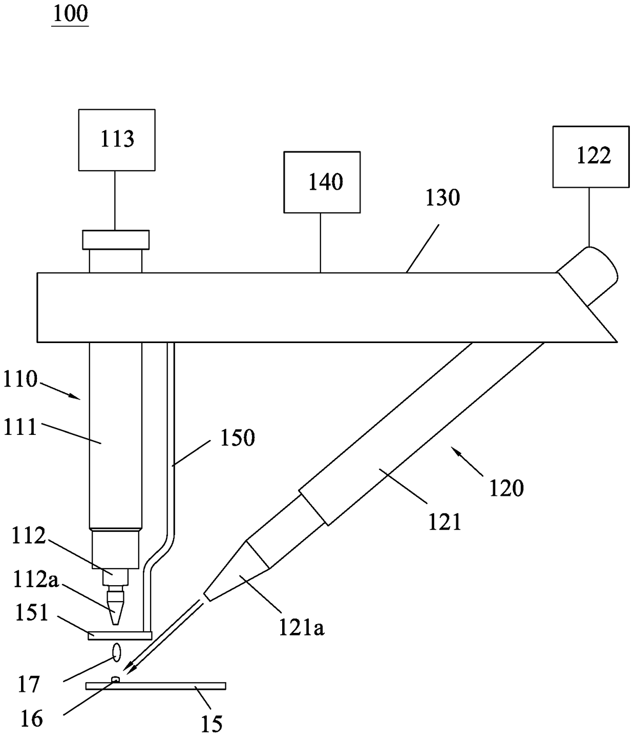
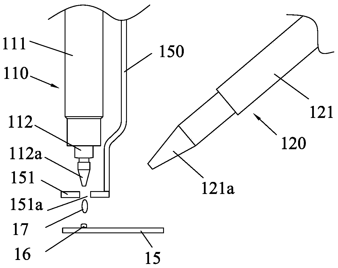
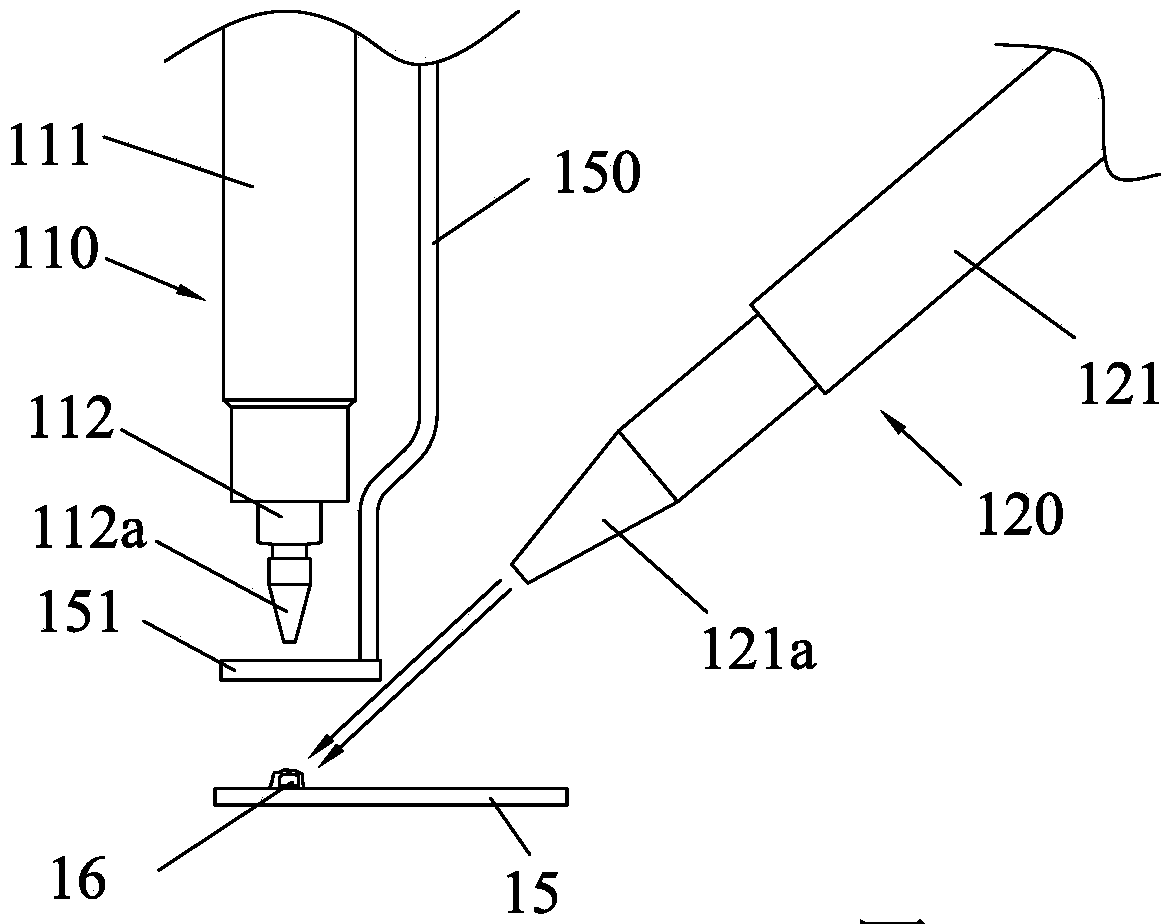
[0023] Several different preferred embodiments of the present invention will now be described with reference to the accompanying drawings, wherein like reference numerals in different drawings represent like parts. As mentioned above, the essence of the present invention lies in a semiconductor processing device and processing method, which has high gluing efficiency, accurate gluing position, and automatic curing treatment after gluing on the glue sprayer, thereby realizing efficient processing. The device and the method are applicable to any semiconductor components that need to be bonded by resin adhesives, and are not limited to the field of disk drives.

[0024] Please refer to figure 1 The semiconductor processing device 100 of the present invention includes a glue sprayer 110 , an ultraviolet light emitting device 120 , and a mounting plate 130 for installing the glue sprayer 110 and the ultraviolet light emitting device 120 . The glue spraying machine 110 in this embo...


PUM


Abstract

The semiconductor processing device of the present invention includes a glue sprayer and an ultraviolet light emitting device installed on a mounting board. The glue spraying machine includes a syringe for accommodating spraying materials, a striker inserted in the syringe and a first control device connected with the striker, the end of the striker is a nozzle protruding from the syringe; the ultraviolet light emitting device includes a The emission end and the second control device for controlling the emission of ultraviolet light, the emission end and the nozzle are arranged on one side of the nozzle at an acute angle, the second control device is connected with the first control device, after the nozzle sprays glue to the spraying area , within a preset time, the emitting end emits ultraviolet light to the spraying area so as to realize the curing of the glue. The gluing machine has high gluing efficiency and accurate gluing position, and the ultraviolet light emitting device automatically performs curing treatment after gluing the gluing machine, so as to achieve efficient processing.

Description

technical field [0001] The invention relates to a device and a method for processing semiconductor products, in particular to a device and a method for spraying and curing glue on a semiconductor surface to be bonded. Background technique [0002] In the production process of semiconductor products, the bonding between parts is often involved, and there are many kinds of adhesives used for bonding, and UV glue has become one of the most widely used at present due to its safety, economy and good compatibility. of adhesives. UV glue is ultraviolet light curing glue, which is composed of base resin, active monomer, photoinitiator and other main components, as well as auxiliary agents such as stabilizer, crosslinking agent and coupling agent. Under the irradiation of ultraviolet light of appropriate wavelength, the photoinitiator quickly generates free agents or ions, and then initiates the polymerization and crosslinking of the base resin and active monomers to form a network ...

Claims


Application Information

Patent Timeline
Patent Type & Authority Patents(China)
IPC IPC(8): B05C5/02B05C11/10B05D1/02B05D3/06H01L21/67
Inventor 高寿生陈灿华
Owner SAE TECH DELEVOPMENT DONGGUAN
Why Eureka
Try Eureka