Array substrate, manufacturing method of array substrate, display panel and display device

A technology of an array substrate and a manufacturing method, which is applied in the field of touch display, can solve the problems of light and thin display devices, many manufacturing processes, and large thickness that are not applicable, and achieve the effects of improving touch sensitivity, reducing manufacturing processes, and reducing resistance

Active Publication Date: 2015-06-24
SHANGHAI TIANMA MICRO ELECTRONICS CO LTD +1
View PDF4 Cites 8 Cited by
  • Summary
  • Abstract
  • Description
  • Claims
  • Application Information

AI Technical Summary

Problems solved by technology

However, in the prior art, a display device integrated with a touch function is usually provided with a touch panel on the surface of the display device, resulting in more manufacturing processes and a larger thickness of the display device integrated with a touch function in the prior art. , not suitable for the development of thinner and lighter display devices

Method used


Image

  • Array substrate, manufacturing method of array substrate, display panel and display device
  • Array substrate, manufacturing method of array substrate, display panel and display device
  • Array substrate, manufacturing method of array substrate, display panel and display device

Examples


Embodiment Construction

[0040] The following will clearly and completely describe the technical solutions in the embodiments of the present invention with reference to the accompanying drawings in the embodiments of the present invention. Obviously, the described embodiments are only some, not all, embodiments of the present invention. Based on the embodiments of the present invention, all other embodiments obtained by persons of ordinary skill in the art without making creative efforts belong to the protection scope of the present invention.

[0041] In the following description, a lot of specific details are set forth in order to fully understand the present invention, but the present invention can also be implemented in other ways different from those described here, and those skilled in the art can do it without departing from the meaning of the present invention. By analogy, the present invention is therefore not limited to the specific examples disclosed below.

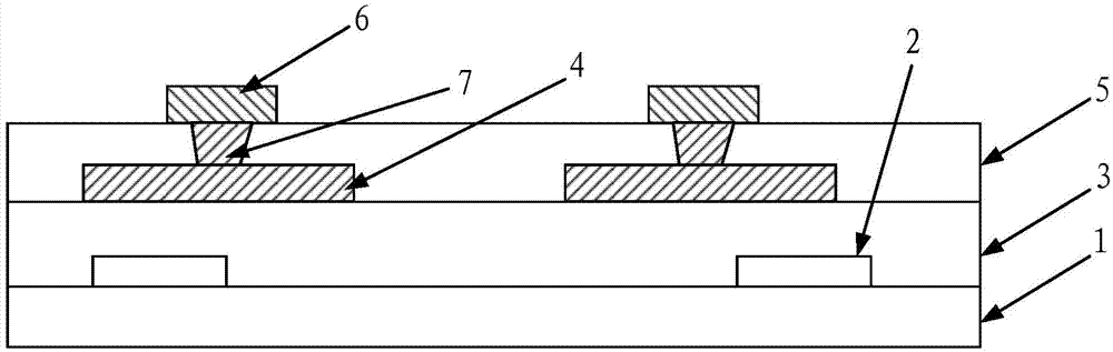
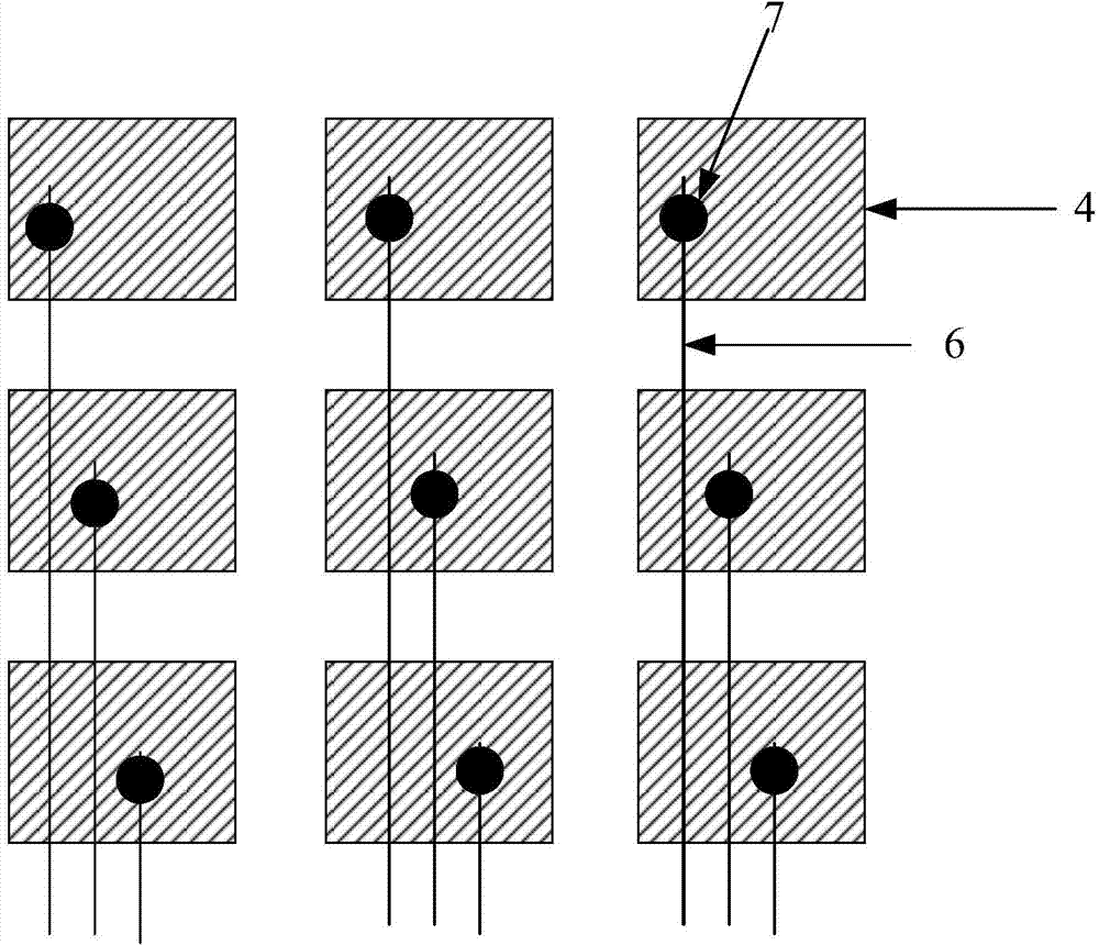
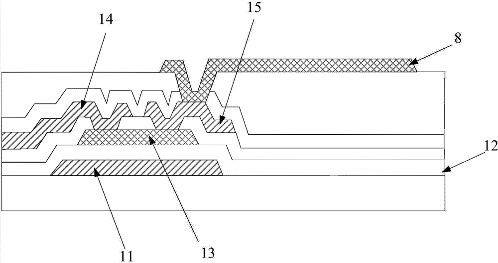
[0042] like figure 1 As shown,...


PUM


Abstract

The embodiment of the invention discloses an array substrate, a manufacturing method of the array substrate, a display panel and a display device. The array substrate comprises a first substrate, a data line layer, a first insulating layer, a first electrode layer, a second insulating layer and a first electrode wiring layer. The first electrode layer comprises a plurality of first electrodes independent from each other. The first electrodes are used as common electrodes during the display stage and used as touch electrodes during the touch stage, and therefore in the array substrate, the display and touch functions can be achieved at the same time only by manufacturing one layer of electrodes; the number of the array substrates and the thickness of the display panel and the display device comprising the array substrates are reduced, the manufacturing procedures of the array substrate, and the display panel and the display device comprising the array substrates are reduced, and the thin and light development of the display device is carried out easily; moreover, in the embodiment, as the first electrodes are metal electrodes, resistance of the first electrodes can be small, the touch sensitivity when the first electrode layer is used as the touch electrodes is remarkably improved.

Description

technical field [0001] The present invention relates to the technical field of touch display, and in particular to an array substrate and a manufacturing method thereof, a display panel including the array substrate, and a display device including the display panel. Background technique [0002] With the development of display technologies, more and more display devices have integrated touch functions. However, in the prior art, a display device integrated with a touch function is usually provided with a touch panel on the surface of the display device, resulting in more manufacturing processes and a larger thickness of the display device integrated with a touch function in the prior art. , not suitable for the development of thinner and lighter display devices. Contents of the invention [0003] In order to solve the above technical problems, embodiments of the present invention provide an array substrate and a manufacturing method thereof, as well as a display panel and...

Claims


Application Information

Patent Timeline
Patent Type & Authority Applications(China)
IPC IPC(8): H01L27/12G06F3/041G02F1/1343H01L21/77
Inventor 孙云刚李谷骏
Owner SHANGHAI TIANMA MICRO ELECTRONICS CO LTD
Why Eureka
Try Eureka