

Array substrate, manufacturing method thereof, display panel and display device
A technology for array substrates and manufacturing methods, which is applied in the fields of instruments, nonlinear optics, optics, etc., can solve the problems such as the reduction of the aperture ratio of array substrates, and achieve the effect of eliminating moiré fringes
- Summary
- Abstract
- Description
- Claims
- Application Information
AI Technical Summary
Problems solved by technology
Method used
Image

Examples
Embodiment Construction
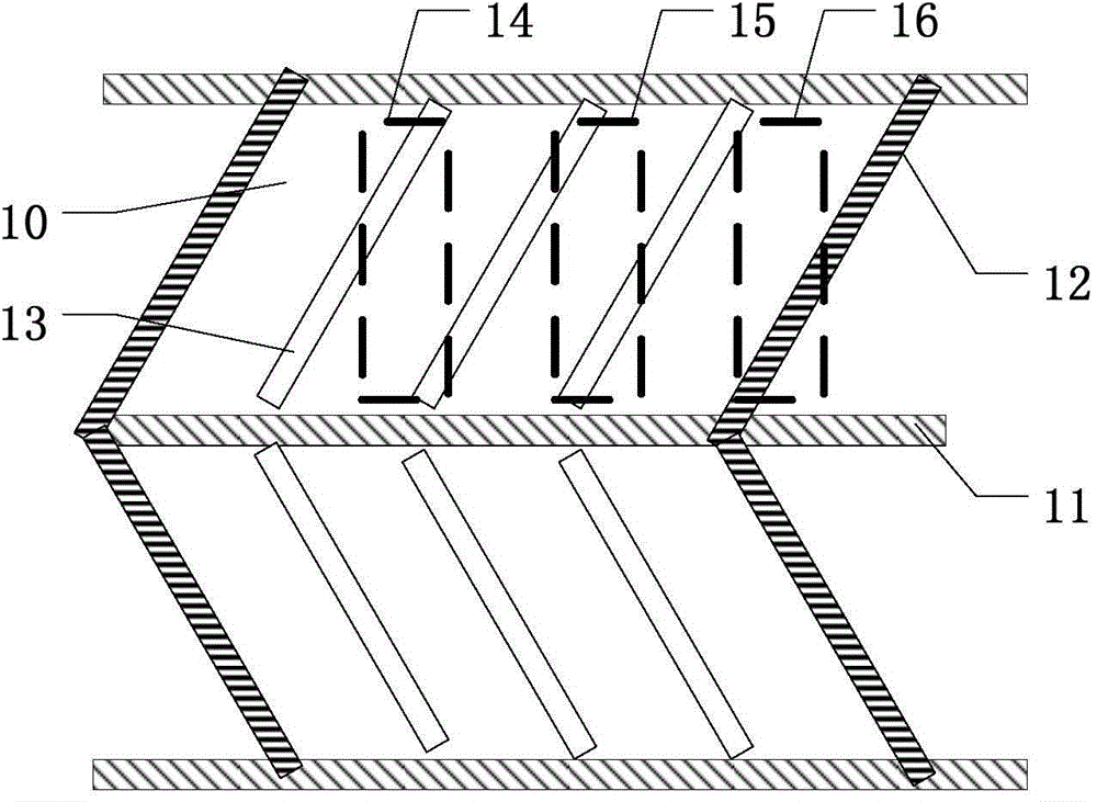
[0038] The present invention will be further described in detail below in conjunction with the accompanying drawings and embodiments. It should be understood that the specific embodiments described here are only used to explain the present invention, but not to limit the present invention. In addition, it should be noted that, for the convenience of description, only some structures related to the present invention are shown in the drawings but not all structures.
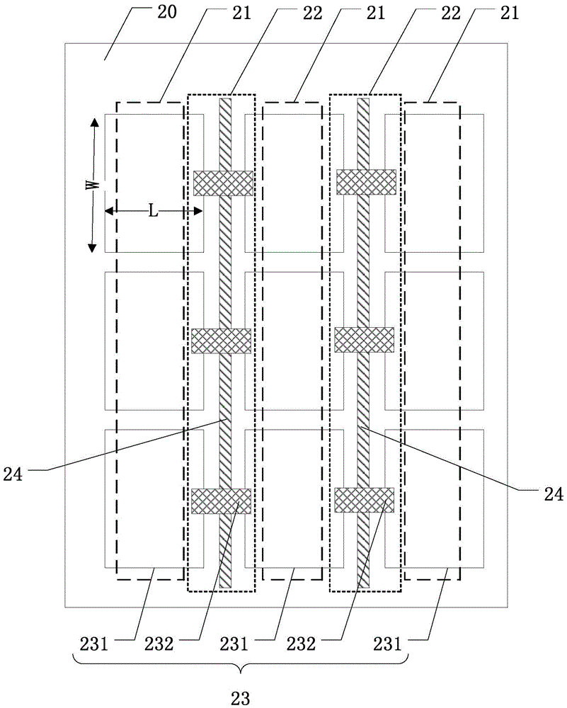
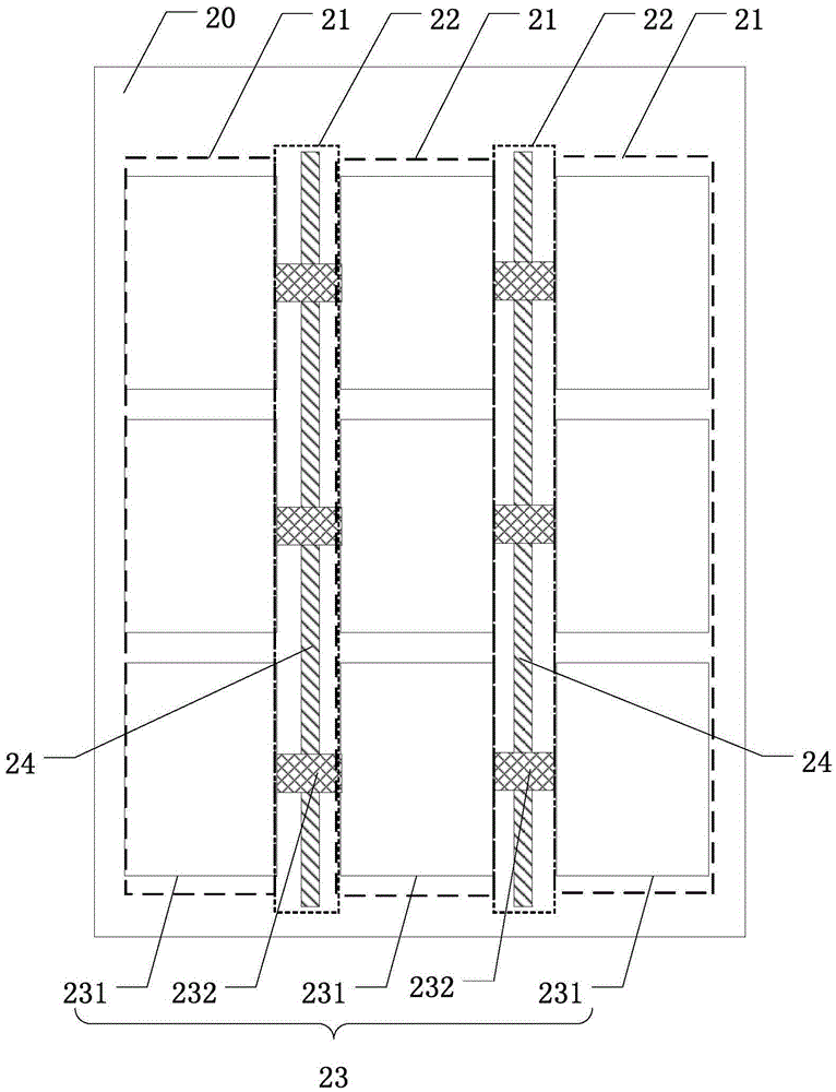
[0039] figure 2 A top view of an array substrate provided for an embodiment of the present invention, such as figure 2 As shown, the array substrate includes: a substrate 20; a plurality of scanning lines 23 and a plurality of data lines 24 that are insulated from each other; wherein each scanning line 23 includes a plurality of transparent conductive parts 231 and a plurality of metal wiring parts 232 , adjacent transparent conductive parts 231 are electrically connected through the metal wiring part 232 . Th...
PUM
 Abstract
Description
Claims
Application Information