Array substrate, display device and wearable device
A technology for an array substrate and a display device, which is applied in the fields of display devices, wearable devices, and array substrates, can solve problems such as low edge display quality, and achieve the effect of solving the problem of low aperture ratio and utilization rate.
- Summary
- Abstract
- Description
- Claims
- Application Information
AI Technical Summary
Problems solved by technology
Method used
Image


Examples
Embodiment 1
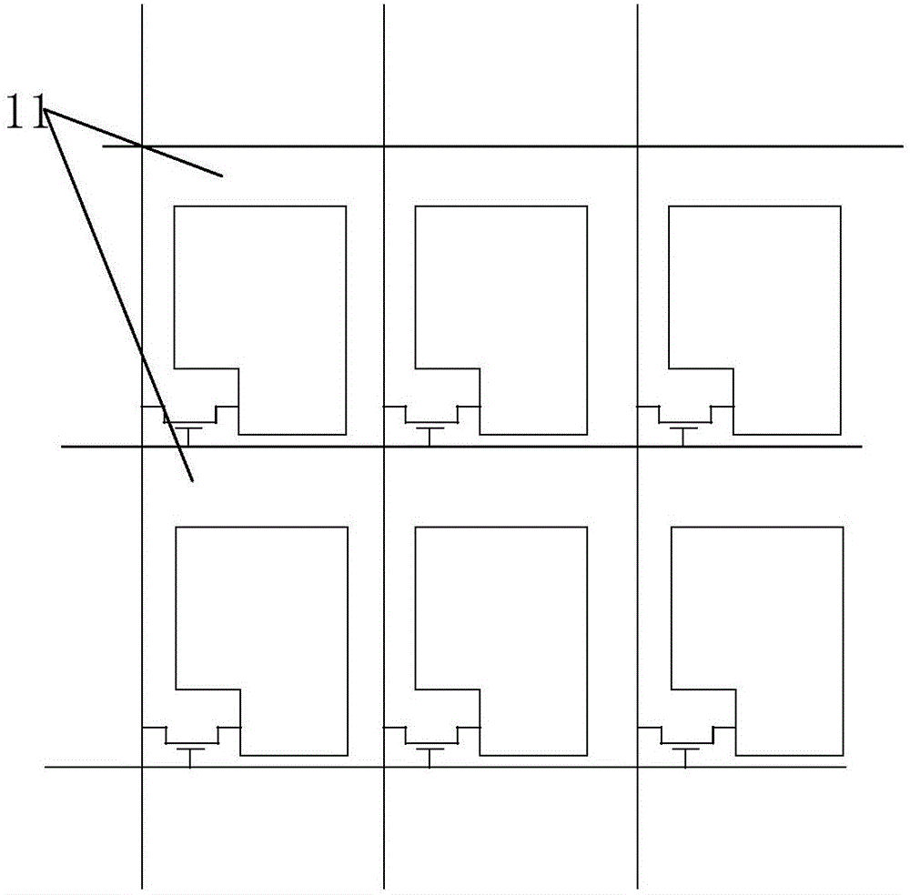
[0034] image 3 It is a schematic structural diagram of the array substrate according to the first embodiment of the present invention. refer to image 3 As shown, the array substrate 10 includes a plurality of pixel units, and the plurality of pixel units form a display area. In the first embodiment, the display area is formed in a circle, that is, a plurality of pixel units are arranged to form a circular display area. Those skilled in the art can understand that each pixel unit includes a thin film transistor and a pixel electrode connected to the thin film transistor, such as figure 1 As shown, the thin film transistors are connected to the data lines and gate lines arranged vertically and horizontally on the array substrate. The arrangement structure of the pixel unit is a conventional technique in the art, and will not be described in detail here.
[0035] refer to image 3 As shown, the array substrate 10 includes at least four setting areas, which are: the first set...
Embodiment 2
[0041] The present invention also provides the array substrate of the second embodiment, wherein on the basis of the first embodiment, the first setting area 110 , the second setting area 120 , the third setting area 130 and the fourth setting area 140 of the array substrate 10 are The combination is formed as the entire display area, such as Image 6 shown.
[0042] see Image 6 As shown, in the second embodiment, the display area is also formed in a circular shape. In the entire display area, the X-axis and Y-axis centerlines of the display area are used as dividing lines, and the entire display area is formed into four display quadrant areas, that is, four setting areas are formed correspondingly.
[0043] Among them, in the first setting area 110, such as Figure 4a As shown, the thin film transistor of each pixel unit is located at the upper left position compared to the pixel electrode; in the second setting area 120, as shown in the figure Figure 4b As shown, the t...
Embodiment 3
[0047] The present invention also provides the array substrate of the third embodiment, wherein in the third embodiment, such as Figure 7 As shown, the array substrate includes a plurality of edge pixel units 12 located at the edge of the display area, wherein the pixel electrode 121 in each edge pixel unit 12 includes a first edge 1211 formed as a part of the edge of the display area, the first edge The 1211 is formed in a curved arc shape, and the thin film transistor 1212 in the edge pixel unit 12 is located on a side closer to the edge of the display area than the pixel electrode 121 . Preferably, the first edges of the pixel electrodes 121 in the plurality of edge pixel units 12 are combined to form the edge of the display area.
[0048] In the array substrate described in the third embodiment, on the basis that the pixel electrodes of the edge pixel units 12 at the edge of the display area are arranged to the side close to the edge of the display area, the pixel electro...
PUM
 Abstract
Description
Claims
Application Information