Patterning method and patterning device

A patterning and process technology, applied in the direction of electrical components, semiconductor/solid-state device manufacturing, circuits, etc., can solve the problems of incomplete etching, short circuit, depth limitation of ion reach, etc., to avoid the effect of etching residues

Inactive Publication Date: 2018-02-13
MACRONIX INT CO LTD
View PDF6 Cites 0 Cited by
  • Summary
  • Abstract
  • Description
  • Claims
  • Application Information

AI Technical Summary

Problems solved by technology

However, the ions used in etching steps such as anisotropic etching have a limit to the depth they can reach, which tends to result in incomplete etching, leaving a ladder-like residue at the bottom of the etched trench
If the above-mentioned ladder-shaped residues are not removed in the subsequent process, there will be abnormal conduction when the device is made, resulting in a short circuit

Method used


Image

  • Patterning method and patterning device
  • Patterning method and patterning device
  • Patterning method and patterning device

Examples


Embodiment Construction

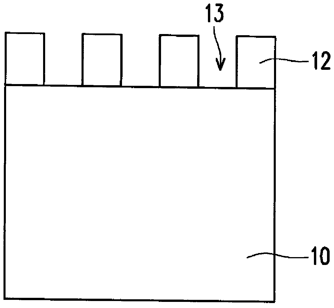
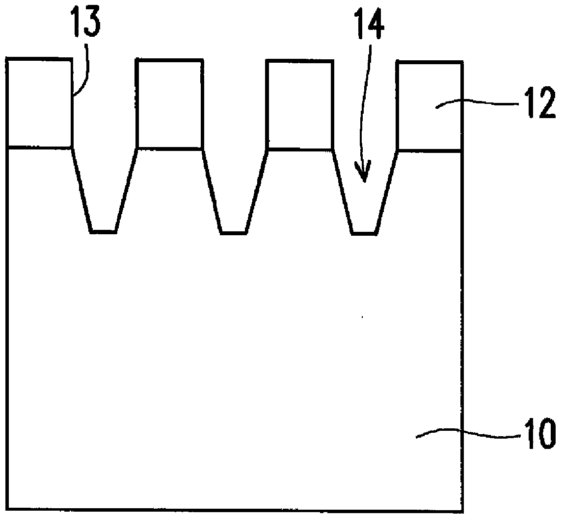
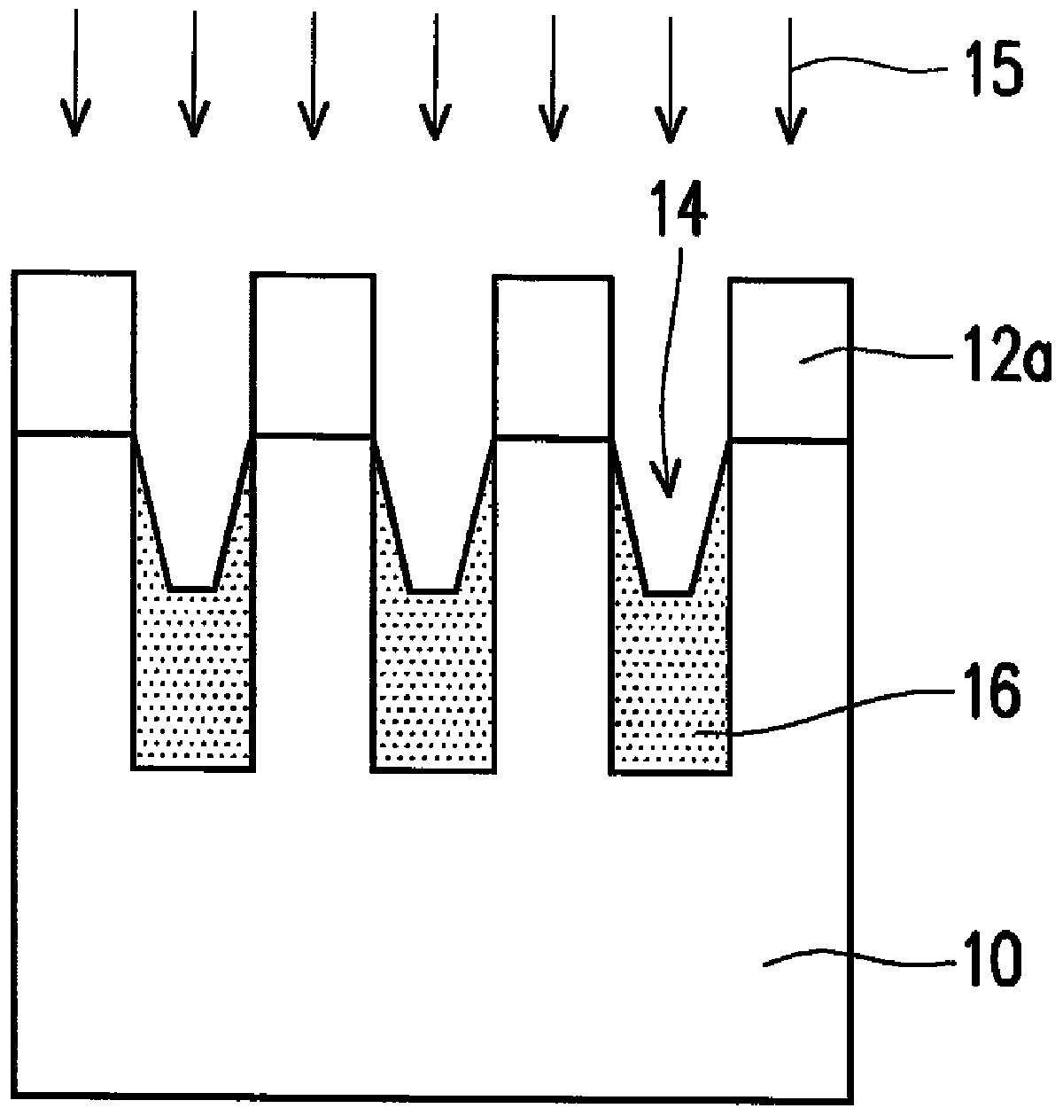
[0059] Figure 1A to Figure 1E It is a schematic cross-sectional view of a patterning method according to an embodiment of the present invention. figure 2 is a flow chart of the patterning method according to the first embodiment of the present invention. image 3 is a flow chart of the patterning method according to the second embodiment of the present invention. Figure 4 is a flow chart of the patterning method according to the third embodiment of the present invention.

[0060] Please refer to Figure 1A and figure 2 , step 102 , forming a patterned mask layer 12 on the material layer 10 . The material layer 10 may be composed of a single material, or may be a stack structure formed by stacking two or more materials. In one embodiment, the material layer 10 may be a semiconductor wafer. The semiconductor wafer is, for example, formed of at least one semiconductor material selected from the group consisting of Si, Ge, SiGe, GaP, GaAs, SiC, SiGeC, InAs and InP. In y...


PUM


Abstract

The invention discloses a patterning method and a patterning device. The patterning method includes: forming a patterned mask layer on a material layer, and the patterned mask layer has a first opening to expose a part of the material layer performing a pretreatment process to modify the exposed material layer of the first opening to form a modified region; performing an etching process to remove the material layer in the modified region to form a second opening.

Description

technical field [0001] The present invention relates to a semiconductor process method and device, and in particular to a patterning method and a patterning device. Background technique [0002] With the increasing demand for high-density memory in the semiconductor industry, such as floating gate memory, charge trapping memory, nonvolatile memory, and embedded memory, the design of memory cells has changed from a planar structure to a three-dimensional structure in order to Increase storage capacity within limited chip area. [0003] In the three-dimensional structure, in order to pursue a higher storage density, the number of stacked layers is continuously increased, so that the aspect ratio of the channel is continuously increased during the etching process. However, the depth that ions used in etching steps such as anisotropic etching can reach is limited, so it is easy to cause incomplete etching and leave ladder-like residues at the bottom of the etched trench. If th...

Claims


Application Information

Patent Timeline
Patent Type & Authority Patents(China)
IPC IPC(8): H01L21/02H01L21/67
Inventor 杨大弘
Owner MACRONIX INT CO LTD
Why Eureka
Try Eureka