Display substrate, display panel cutting method and display device
A technology for display substrates and display panels, which is applied in the fields of instruments, nonlinear optics, optics, etc., can solve the problems of reducing product yield, excessive overlapping area, affecting the flatness of display substrates, etc., and achieves the effect of high product yield.
- Summary
- Abstract
- Description
- Claims
- Application Information
AI Technical Summary
Problems solved by technology
Method used
Image
Examples
Embodiment Construction
[0038] Reference will now be made in detail to the exemplary embodiments, examples of which are illustrated in the accompanying drawings. When the following description refers to the accompanying drawings, the same numerals in different drawings refer to the same or similar elements unless otherwise indicated. The implementations described in the following exemplary examples do not represent all implementations consistent with the present invention. Rather, they are merely examples of apparatuses and methods consistent with aspects of the invention as recited in the appended claims.
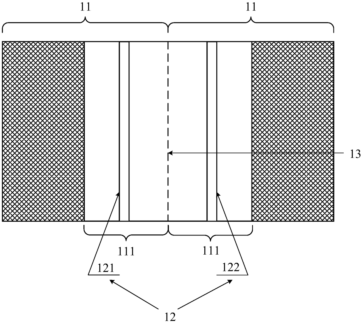
[0039] figure 1 It is a schematic structural diagram of a display substrate shown in an embodiment of the present invention. The display substrate may include:
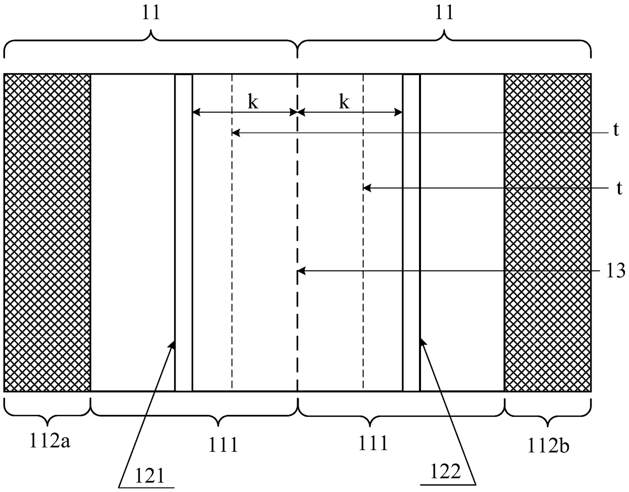
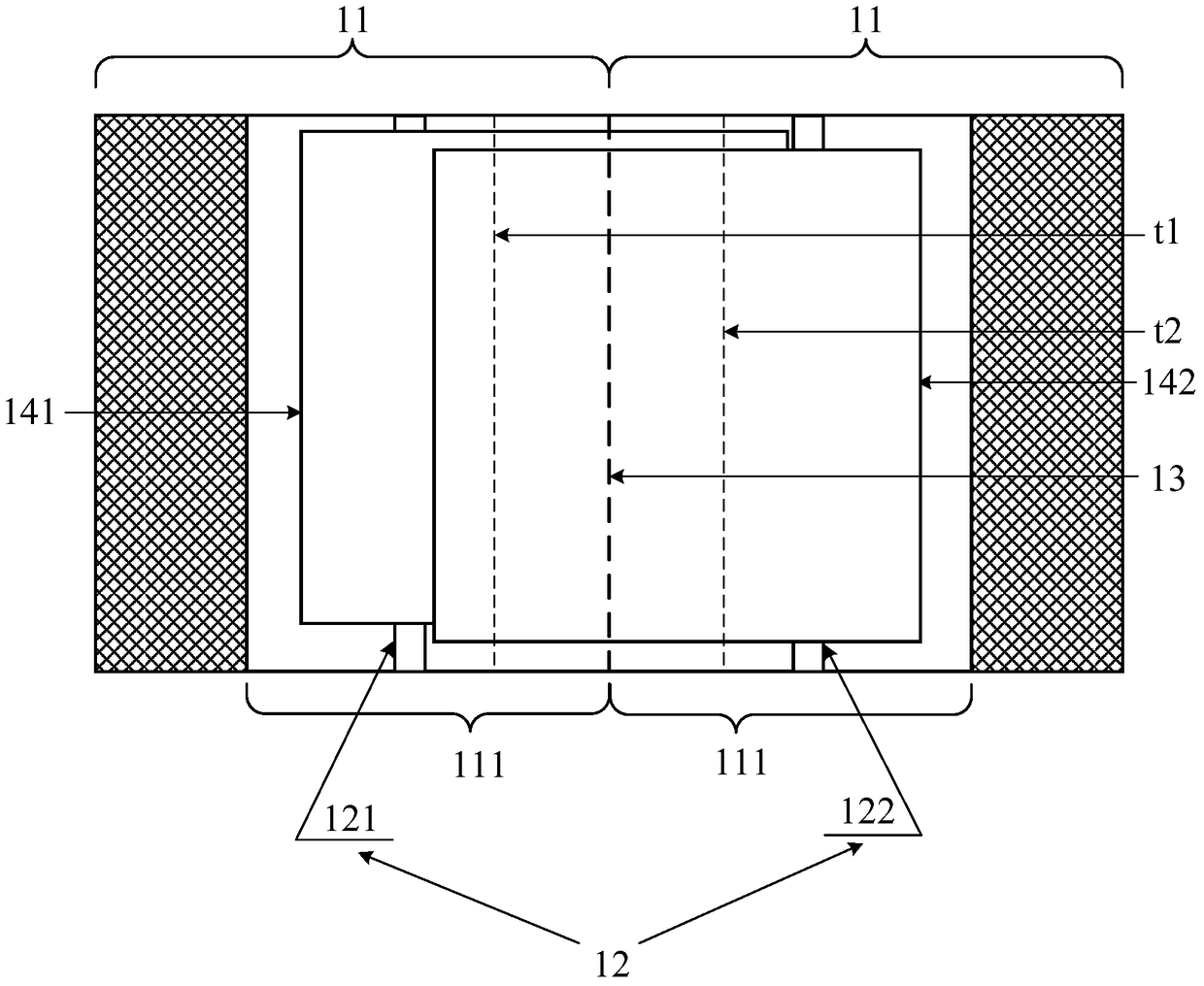
[0040] At least two sub-display regions 11 and at least one barrier unit 12, the sub-display regions 11 are used to form a sub-display substrate.
[0041] Each blocking unit 12 includes: two strip-shaped blocking patterns 121 and 122...
PUM
 Abstract
Description
Claims
Application Information


