System and method for testing radio frequency wireless signal transceivers using wireless test signals
A technology of signal transceiver and test signal, applied in signal transmission system, transmission system, antenna radiation pattern and other directions, can solve the problem that the casing cannot produce measurement accuracy and repeatability.
Inactive Publication Date: 2016-01-27
LITEPOINT
View PDF13 Cites 7 Cited by
- Summary
- Abstract
- Description
- Claims
- Application Information
AI Technical Summary
Problems solved by technology
However, such housings typically do not yield c
Method used
View moreImage
Smart ImageViewing Examples

Examples
 PUM
 Abstract
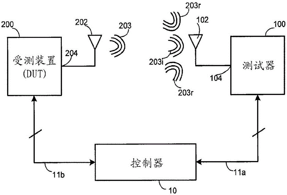
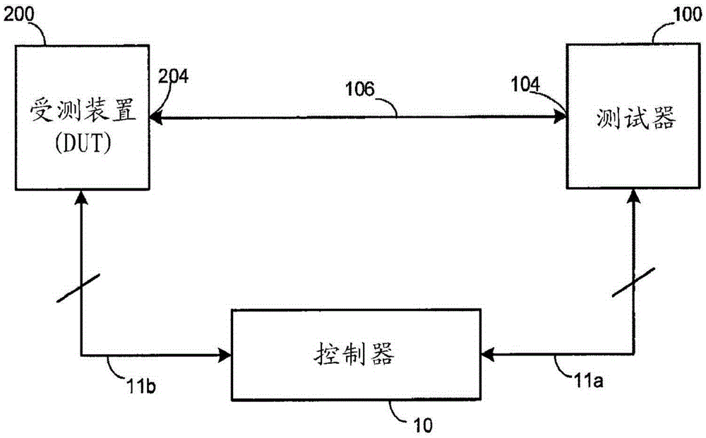
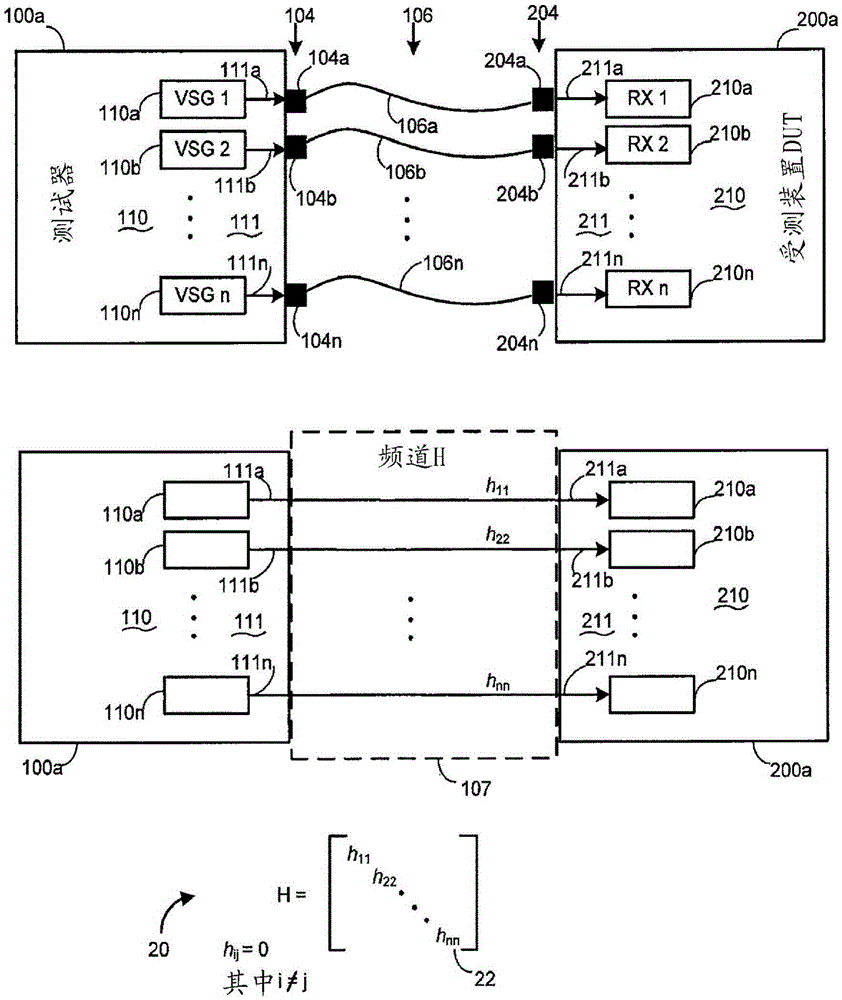
A method for facilitating wireless testing of a radio frequency (RF) signal transceiver device under test (DUT). Using multiple antennas within a shielded enclosure containing the DUT, multiple wireless RF test signals resulting from a RF test signal radiated from the DUT are captured and their respective signal phases are controlled prior to being combined to form a composite RF signal. This process is repeated until power level differences between signal power levels at respective pairs of a selected number of RF signal frequencies have values between predetermined minimum and maximum values, thereby providing compensation for the multipath signal environment within the shielded enclosure, and thereby simulating a wired test signal path during wireless testing of the DUT.
Description
technical field [0001] This patent application is a continuation in part of U.S. Patent Application 13 / 839,162 filed on March 15, 2013 and entitled "System and Method for Testing Radio Frequency Wireless Signal Transceivers Using Wireless Test Signals" (System and Method for Testing Radio Frequency Wireless Signal Transceivers Using Wireless Test Signals), and 2013 Continuation-in-Part of U.S. Patent Application 13 / 839,583, filed March 15 and entitled "System and Method for Testing Radio Frequency Wireless Signal Transceivers Using Wireless Test Signals," the contents of which are incorporated by reference into this article. Background technique [0002] The present invention relates to testing radio frequency (RF) wireless signal transceivers, and more particularly to testing such devices without the use of RF signal cables that transmit RF test signals. [0003] Many of today's electronic devices use wireless technology for both connection and communication purposes. Bec...
Claims
Login to View More Application Information
Patent Timeline
 IPC IPC(8): G01R29/10G08C17/04
CPCH04B17/3911G01R29/10
Inventor 明-乔·忽恩
Owner LITEPOINT
Features
- R&D
- Intellectual Property
- Life Sciences
- Materials
- Tech Scout
- Unparalleled Data Quality
- Higher Quality Content
- 60% Fewer Hallucinations
Learn More Browse by: Latest US Patents, China's latest patents, Technical Efficacy Thesaurus, Application Domain, Technology Topic, Popular Technical Reports.
© 2025 PatSnap. All rights reserved.Legal|Privacy policy|Modern Slavery Act Transparency Statement|Sitemap|About US| Contact US: help@patsnap.com