Chip section polishing device and polishing method

A polishing device and chip technology, applied in the direction of grinding device, grinding machine tool, working carrier, etc., can solve the problems of complicated operation, manpower consumption, time waste, etc., and achieve the effect of observation

Active Publication Date: 2018-06-26
WUHAN XINXIN SEMICON MFG CO LTD
View PDF6 Cites 0 Cited by
  • Summary
  • Abstract
  • Description
  • Claims
  • Application Information

AI Technical Summary

Problems solved by technology

[0004] This device completes the polishing operation of different sections of the chip by removing the chip, then turning it in one direction and fixing the chip on the device body again. This method is complicated to operate, resulting in unnecessary waste of time and more labor-intensive

Method used


Image

  • Chip section polishing device and polishing method
  • Chip section polishing device and polishing method
  • Chip section polishing device and polishing method

Examples


Embodiment Construction

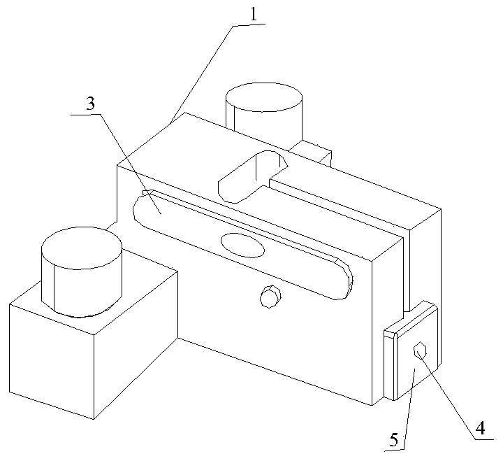
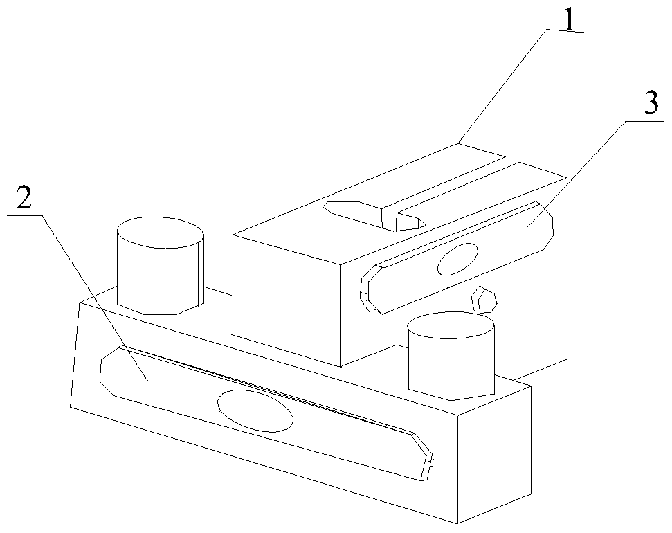
[0033] The invention provides a chip section polishing device, see figure 1 and figure 2 As shown, the device includes a device body 1, a card slot is arranged on the device body 1, and two levels are provided at the same time, respectively 2 and 3, wherein the level 3 is arranged on the surface adjacent to the surface where the card slot is located, and the level 2 is arranged on the surface adjacent to the level 3 and different from the surface where the card slot is located, that is, the level 2 is arranged on the surface opposite to the plane where the card slot is located on the device body.

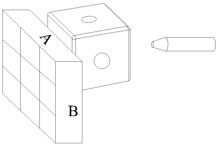
[0034] This chip interface polishing device comprises a chip carrier 5, and this chip carrier 5 is arranged as cube structure, and each face of chip carrier is all provided with a through hole, and the through hole of each face and the through hole of the face opposite to this face of chip carrier Connected, and form a connected through hole 4, at the same time, each side of the c...


PUM


Abstract

The present invention relates to the technical field of semiconductor equipment manufacturing, in particular to a chip cross-section polishing device and a polishing method. By constructing a chip cross-section polishing device including a device body and a chip carrier, two levels are arranged in the device body and the chip carrier is set as A cube structure with a through hole, fix the chip carrier with the chip attached to the card slot of the device body, turn over and polish all adjacent surfaces of the chip, after the polishing operation is completed, remove the chip carrier, and insert the rotating handle into the through hole hole, control the position of the rotating handle, and observe the various angles of the chip. This technical solution can quickly and flexibly realize the polishing operation on the adjacent cross-section of the chip, eliminating the need to repeatedly fix / remove the chip in the traditional technical solution. At the same time, the cube carrier with through holes can be directly used as the carrier of the scanning electron microscope, and at the same time, it can realize the 3D observation effect of the sample.

Description

technical field [0001] The invention relates to the technical field of manufacturing semiconductor equipment, in particular to a chip section polishing device and a polishing method. Background technique [0002] The traditional chip cross-section polishing device fixes the chip on the cylindrical chip carrier when polishing the chip, and exposes the surface of the chip that needs to be observed by grinding. After the grinding is completed, the chip is removed from the chip carrier. Put it into a SEM (Scanning Electron Microscope, scanning electron microscope, referred to as SEM) for the next step of observation. [0003] This method can complete the polishing of the chip and the observation after polishing. However, this polishing device can only process one cross section of the chip at a time. If two or more cross sections of the chip to be observed need to be observed, it is necessary to first One section of the chip is ground to the target position, and then the adjacen...

Claims


Application Information

Patent Timeline
Patent Type & Authority Patents(China)
IPC IPC(8): B24B37/30B24B37/10
CPCB24B37/042B24B37/10B24B37/30
Inventor 肖科仝金雨李桂花谢渊郭伟
Owner WUHAN XINXIN SEMICON MFG CO LTD
Why Eureka
Try Eureka