Pixel compensation circuit and amoled display device

A technology for compensating circuits and pixels, applied to static indicators, instruments, etc., can solve the problems of poor uniformity of pixel brightness and uneven display, so as to improve uniformity of brightness, avoid changes in brightness, and improve display effect and display uniformity Effect

Active Publication Date: 2018-04-06
BOE TECH GRP CO LTD +1
View PDF6 Cites 0 Cited by
  • Summary
  • Abstract
  • Description
  • Claims
  • Application Information

AI Technical Summary

Problems solved by technology

[0006] In the above-mentioned AMOLED display device, the organic light emitting diode D is driven according to the current generated by the second transistor T2 in a saturated state; and due to the unevenness of the TFT manufacturing process, the threshold voltage of the second transistor T2 in each pixel is different, and, due to the second transistor T2 The threshold voltage Vth of the second transistor T2 will drift to different degrees during the light-emitting process of the organic light-emitting diode D. When the above-mentioned 2T1C driving circuit is used for driving, the brightness uniformity of each pixel is very poor, resulting in uneven display.

Method used


Image

  • Pixel compensation circuit and amoled display device
  • Pixel compensation circuit and amoled display device
  • Pixel compensation circuit and amoled display device

Examples


Embodiment Construction

[0028] Specific embodiments of the present invention will be described in detail below in conjunction with the accompanying drawings. It should be understood that the specific embodiments described here are only used to illustrate and explain the present invention, and are not intended to limit the present invention.

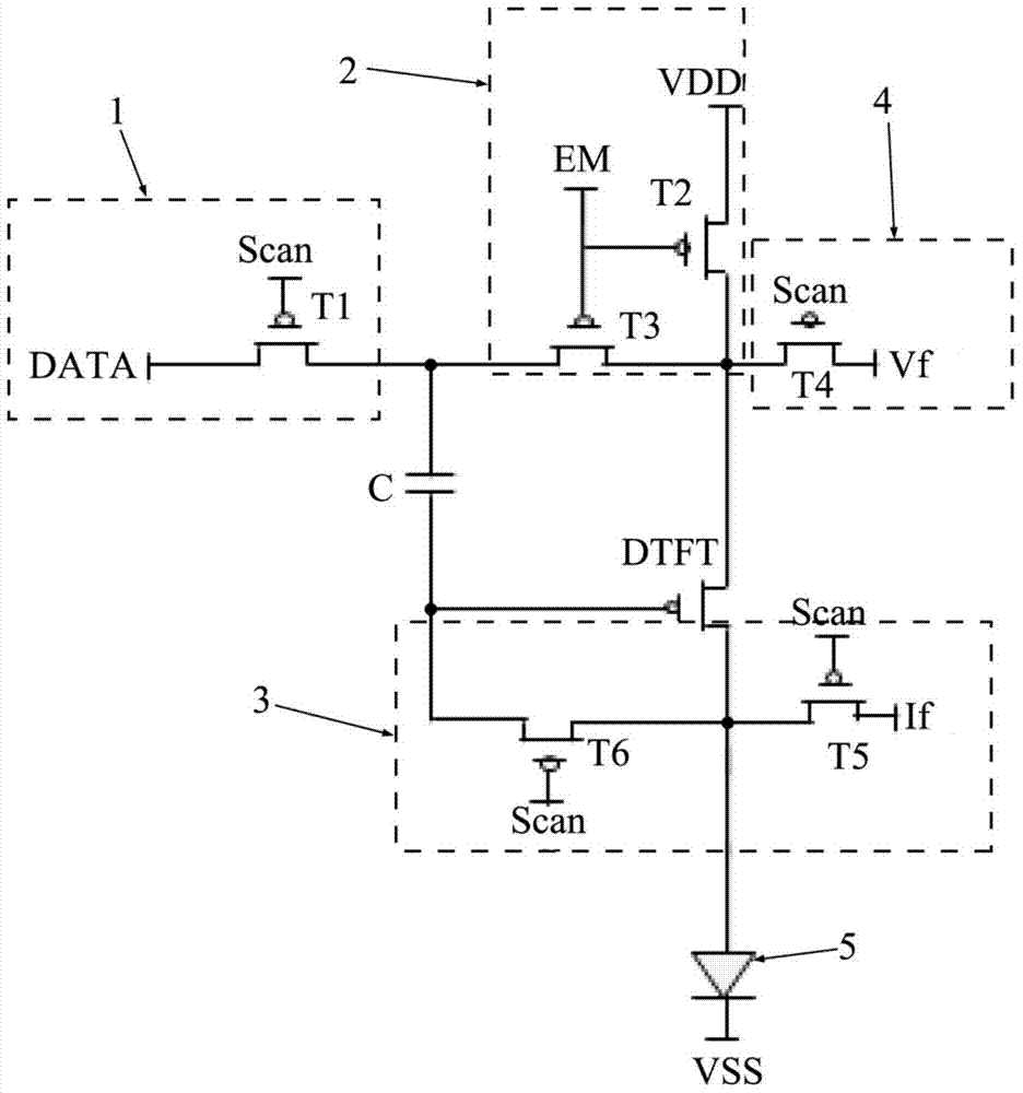
[0029] The present invention provides multiple implementations of a pixel compensation circuit. figure 2 It is a circuit diagram of the pixel compensation circuit in the first embodiment of the present invention. Such as figure 2 As shown, in this embodiment, the pixel compensation circuit includes a data signal writing module 1, a high voltage signal writing module 2, a first reference voltage generating module 3, a second reference voltage writing module 4, a driving transistor DTFT , capacitor C and light emitting device 5 . The data signal writing module 1 is connected to the first end of the capacitor C before the light-emitting device 5 emits light; t...


PUM


Abstract

A pixel compensation circuit and an Active Matrix Organic Light Emitting Diode (AMOLED) display apparatus. The circuit includes a data signal writing module, a high voltage signal writing module, a first reference voltage generation module and a second reference voltage writing module; the data signal writing module and the high voltage signal writing module are connected with a first terminal of the capacitor; the first reference voltage generation module is connected with a second terminal of the capacitor and a drain of the driving transistor; a gate of the driving transistor is connected with the second terminal of the capacitor, the drain thereof is connected with an anode of the light emitting device, a source thereof is connected with the second reference voltage writing module, and connected with the high voltage signal writing module; a cathode of the light emitting device is connected with a common ground electrode.

Description

technical field [0001] The present invention relates to the field of display technology, in particular to a pixel compensation circuit and an AMOLED display device. Background technique [0002] The flat panel display device has many advantages such as thin body, power saving, and no radiation, and thus has been widely used. Existing flat panel display devices mainly include liquid crystal display (Liquid Crystal Display, hereinafter referred to as LCD) and organic light emitting diode (Organic Light Emitting Diode, hereinafter referred to as OLED) display devices. [0003] The OLED display device achieves display through self-luminescence, so it does not require a backlight source, and has high contrast, small thickness, wide viewing angle, fast response speed, can be made into a flexible display panel, wide operating temperature range, and relatively simple structure and manufacturing process. characteristics, it is regarded as a next-generation display device that can re...

Claims


Application Information

Patent Timeline
Patent Type & Authority Patents(China)
IPC IPC(8): G09G3/3258
CPCG09G3/3233G09G3/20G09G3/3225G09G3/3258G09G3/3266G09G2300/0814G09G2300/0819G09G2300/0842
Inventor 何小祥祁小敬
Owner BOE TECH GRP CO LTD
Why Eureka
Try Eureka