Method for forming grid

A gate and layer-forming technology, applied in the field of gate formation, to achieve the effect of reducing bridging problems, smooth surface, and highly consistent

Active Publication Date: 2016-03-30
SEMICON MFG INT (SHANGHAI) CORP
View PDF6 Cites 3 Cited by
  • Summary
  • Abstract
  • Description
  • Claims
  • Application Information

AI Technical Summary

Problems solved by technology

[0006] However, transistors formed in the gate-last process have the problem of being easy to bridge with other devices

Method used


Image

  • Method for forming grid
  • Method for forming grid
  • Method for forming grid

Examples


Embodiment Construction

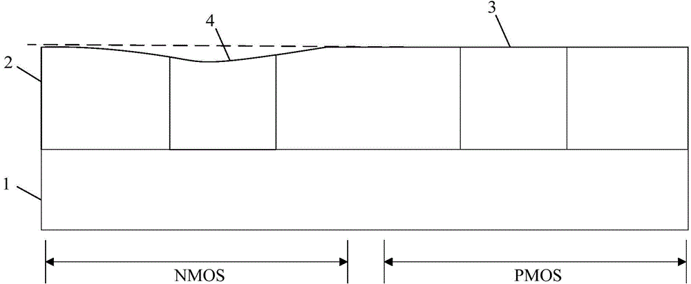
[0041] In order to solve the problem of easy bridging between transistors and other devices, each step of the gate-last process is analyzed. When chemical mechanical polishing (CMP) is used to remove unnecessary parts of the metal layer, due to the (being) polished between different materials There can be large differences in the rate (RR), which can lead to height differences between the different materials after CMP, causing bridging problems.

[0042] Specifically, refer to figure 1 , the manufacture of CMOS devices requires the gates of PMOS and NMOS devices to be formed separately. Taking the metal gate 3 of the PMOS device formed first as an example, when the metal gate 3 of the PMOS device is formed by chemical mechanical polishing, there is still a dummy gate 4 to be removed in the NMOS device at this time.

[0043] Although in general, the chemical mechanical polishing of the metal gate 3 of the PMOS device stops when the interlayer dielectric layer 2 is detected, th...


PUM

PropertyMeasurementUnit
thicknessaaaaaaaaaa

Abstract

The invention provides a method for forming a grid, and the method comprises the steps: providing a substrate, and enabling the substrate to be provided with a first region and a second region; forming a pseudo grid and an interlayer dielectric layer; forming a sacrificial layer; removing the pseudo grid in the first region, so as to form a first opening in the interlayer dielectric layer in the first region; forming first metal layers on the surface of the sacrificial layer in the second region, the surface of the interlayer dielectric layer in the first region and in the first opening; and removing a part of the first metal layers and a part of the sacrificial layer through chemical mechanical grinding, so as to form the first grid. The beneficial effects of the invention lies in that the pseudo grid in the second region is enabled not to be exposed in the process of chemical mechanical grinding, and a problem of sinking caused by the excessive removal of the pseudo grid in the second region through the chemical mechanical grinding is solved, thereby enabling a surface formed by the pseudo grid and the interlayer dielectric layer to be flatter and more consistent in height, and facilitating the reduction of possible bridging during the subsequent forming of the grid.

Description

technical field [0001] The invention relates to the field of semiconductor manufacturing, in particular to a method for forming a gate. Background technique [0002] Complementary Metal Oxide Semiconductor (CMOS) is the basic unit in modern logic circuits, including PMOS and NMOS devices. [0003] Both the PMOS and NMOS devices are composed of a gate (Gate), a P-type or N-type source region (Source) region or a drain region (Drain) region located in the substrate on both sides of the gate, and a drain region located between the source region and the drain region. The channel (Channel) constitutes. [0004] With the development of semiconductor technology, the gate-last process (gate-last) is gradually used in the prior art to form the gate of semiconductor devices. This process generally forms a dummy gate (dummy gate) first, then forms a source region and a drain region, and then Covering the interlayer dielectric layer, removing the dummy gate to form an opening in the i...

Claims


Application Information

Patent Timeline
Patent Type & Authority Applications(China)
IPC IPC(8): H01L21/28H01L21/8238
Inventor 蒋莉黎铭琦
Owner SEMICON MFG INT (SHANGHAI) CORP
Why Eureka
Try Eureka