Method for fabricating characters on thick copper board of PCB

A thick copper plate and character technology, applied in the secondary processing of printed circuits, electrical components, printed circuits, etc., can solve problems such as unclear characters, improve appearance quality, reduce the difficulty of silk screen printing, and improve the effect of silk screen printing quality.

Active Publication Date: 2016-04-13
JIANGMEN SUNTAK CIRCUIT TECH
View PDF5 Cites 6 Cited by
  • Summary
  • Abstract
  • Description
  • Claims
  • Application Information

AI Technical Summary

Problems solved by technology

[0003] The present invention aims at the problem that the characters on the base material near the copper surface tend to be unclear when making characters on the PCB thick copper plate in the prior art, and provides a character making method that can prevent the characters from being unclear on the PCB thick copper plate

Method used

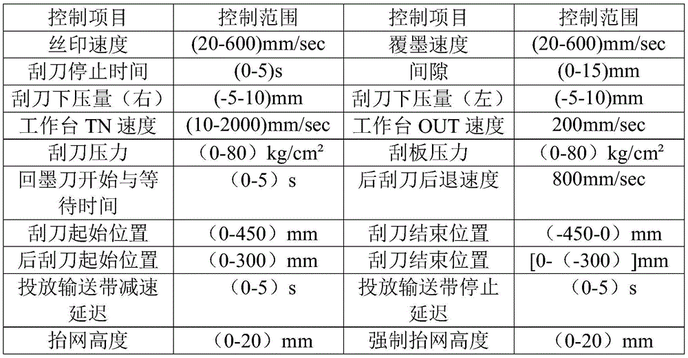

Image

  • Method for fabricating characters on thick copper board of PCB

Examples


Embodiment

[0018] This embodiment provides a method for making characters on a PCB thick copper board, which mainly divides the silk screen printing process into two times, and respectively screens the characters on the substrate surface and the characters on the copper surface, and makes any character on the production board It is not printed on the substrate surface and the copper surface at the same time, and the characters are silk-screen printed on the copper surface of the production board as much as possible. Specific steps are as follows:

[0019] (1) Production board

[0020] According to the existing technology, the inner layer circuit is made by cutting → negative film process → pressing → drilling → copper sinking → full board electroplating → outer layer pattern transfer → pattern electroplating → film fading, etching → tin stripping → silk screen solder mask, The base material is made into a production board with outer layer wiring and solder mask made.

[0021] (2) Subst...


PUM


Abstract

The invention relates to the technical field of production of circuit boards, in particular to a method for fabricating characters on a thick copper board of a PCB. According to the method, screens for a substrate surface and a copper surface are designed respectively, so that the condition that a single character is partially located on the substrate surface and partially located on the copper surface is avoided. The characters on the substrate surface and the copper surface are silkscreened twice respectively, so that the problem that no ink is formed on the substrate close to the copper surface due to large ladder heights of the copper surface and the substrate surface in a conventional design is solved; the problem of excessive ink on the copper surface caused by excessive pressure of primary screen printing or the problem of absence of the ink on the substrate surface caused too small pressure of primary screen printing can also be avoided through twice screen printing; clear characters can be fabricated on the thick copper board of the PCB; and the appearance quality of a product is improved. Meanwhile, specific screens and screen printing parameters are used cooperatively, so that the screen printing quality can be ensured; and the quality of the characters is ensured.

Description

technical field [0001] The invention relates to the technical field of circuit board production, in particular to a method for making characters on a PCB thick copper board. Background technique [0002] According to different design requirements, the copper layer thickness (copper surface thickness) of the outer layer circuit on the PCB will be different. Some PCBs require the copper layer thickness of the outer layer circuit to be ≥ 70 μm. This type of PCB is called PCB thick copper board. The existing PCB production process is generally to make the outer circuit on the multi-layer board, then make the solder mask on the surface of the multi-layer board, and then make characters in a certain area, as follows: the previous process makes the outer circuit Multi-layer board → silk screen solder resist ink → pre-baking → alignment exposure → development → QC inspection board → silk screen character ink → curing → QC inspection board → post-process. In the production process o...

Claims


Application Information

Patent Timeline
Patent Type & Authority Applications(China)
IPC IPC(8): H05K3/22
CPCH05K3/22H05K2201/09936
Inventor 钟宇玲陈广龙胡志勇罗家伟
Owner JIANGMEN SUNTAK CIRCUIT TECH
Why Eureka
Try Eureka