Array substrate and display panel
A technology for array substrates and display areas, which is applied in the fields of instruments, computing, and electrical digital data processing, etc. It can solve the problems of aggravating display defects, eliminating resistance differences, and top defects, etc., and achieves the effect of improving display effects and improving test accuracy
- Summary
- Abstract
- Description
- Claims
- Application Information
AI Technical Summary
Problems solved by technology
Method used
Image
Examples
Embodiment Construction
[0029] Example embodiments will now be described more fully with reference to the accompanying drawings. Example embodiments may, however, be embodied in many forms and should not be construed as limited to the embodiments set forth herein; rather, these embodiments are provided so that this disclosure will be thorough and complete, and will fully convey the concept of example embodiments to those skilled in the art. The same reference numerals denote the same or similar structures in the drawings, and thus their repeated descriptions will be omitted.
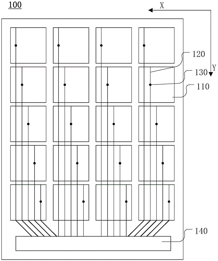
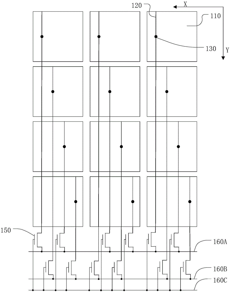
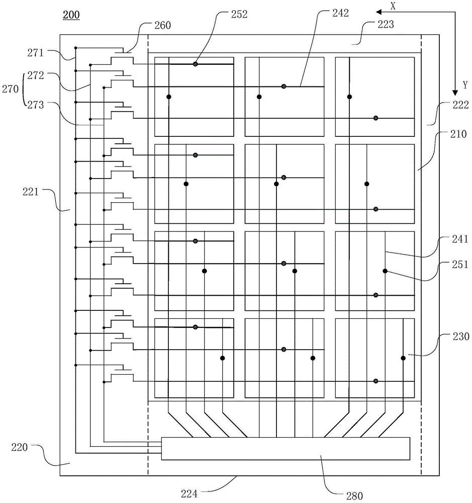
[0030] In order to solve the defect of poor display of the display panel in the prior art, the present invention provides an array substrate. The array substrate includes a display area and a frame area surrounding the display area. The display area is provided with a common electrode layer, a touch wiring layer and a gate layer. The common electrode layer includes a plurality of common electrode units, the touch trace layer...
PUM
 Abstract
Description
Claims
Application Information


