Thin film transistor substrate and display device including same

A technology of thin film transistors and substrates, applied in the direction of transistors, semiconductor devices, electric solid devices, etc., can solve the problems of high power consumption, insufficient charging of panel capacitance, etc., and achieve the effect of reducing series impedance, solving insufficient charging, and avoiding the drop of turn-on current

Active Publication Date: 2018-11-06
INNOLUX CORP
View PDF3 Cites 0 Cited by
  • Summary
  • Abstract
  • Description
  • Claims
  • Application Information

AI Technical Summary

Problems solved by technology

[0007] Another object of the present invention is to provide a display device that can solve the problems of insufficient charging of panel capacitance and excessive power consumption.

Method used


Image

  • Thin film transistor substrate and display device including same
  • Thin film transistor substrate and display device including same
  • Thin film transistor substrate and display device including same

Examples


Embodiment 1

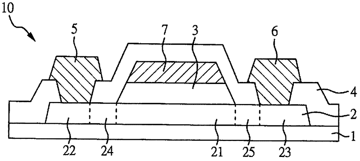
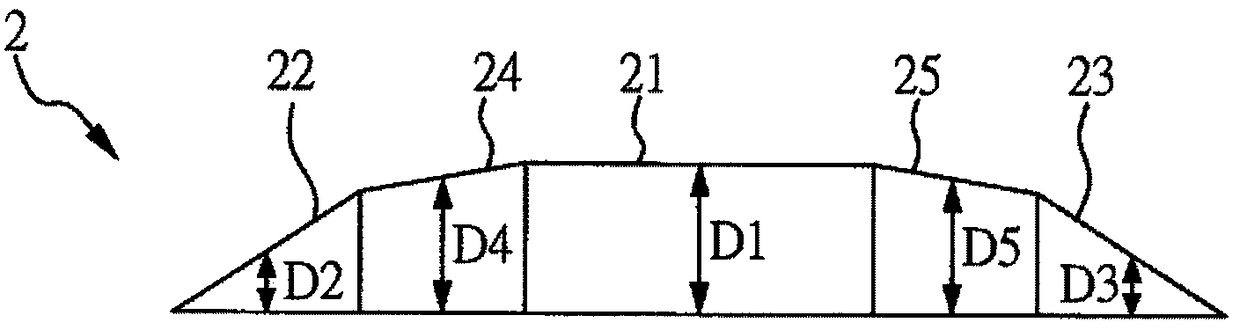
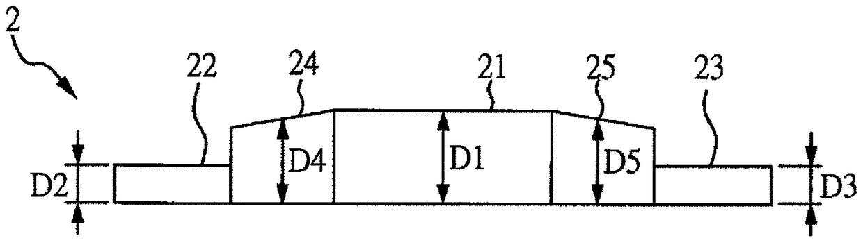
[0027] Please refer to figure 1 , the present invention provides a thin film transistor substrate 10, comprising: a base layer 1; a semiconductor layer 2 disposed on the base layer 1; a first insulating layer 3, a second insulating layer 4, a source electrode 5 and a Drain electrodes 6 are disposed on the semiconductor layer 2 ; and a gate electrode 7 is disposed on the base layer 1 and corresponds to the semiconductor layer 2 . Wherein, the semiconductor layer 2 includes a first region 21, a second region 22 and a third region 23, the first region 21 corresponds to the gate electrode 7, and the second region 22 corresponds to the source electrode 5 , and the third region 23 is corresponding to the drain electrode 6, wherein, figure 2 Shown is an enlarged view of the semiconductor layer 2, the first region 21 has a first thickness D1, the second region 22 has a second thickness D2, the third region has a third thickness D3, and the first The thickness D1 is larger than the ...

Embodiment 2

[0038] The present invention further provides a display device, comprising: the thin film transistor substrate, a pair of side substrates disposed on the thin film transistor substrate; and a display unit disposed between the thin film transistor substrate and the opposite side substrates. Such as Image 6 As shown, when the display device of the present invention is a liquid crystal display device (LCD), it also includes a liquid crystal unit 20 and a color filter substrate 30 disposed above the thin film transistor substrate 10, and a backlight module disposed below the thin film transistor substrate 10 40; or, if Figure 7 As shown, when the display device of the present invention is an organic light emitting diode device (OLED), it also includes an organic light emitting diode 50 and a packaging substrate (or thin film packaging module) 60 disposed above the thin film transistor substrate 10 . In addition, those skilled in the art can easily understand other omitted compo...


PUM


Abstract

The invention relates to a thin film transistor substrate, which comprises a basic layer, a semiconductor layer, a source electrode, a drain electrode, and a gate electrode, wherein the semiconductor layer is arranged on the basic layer; the source electrode and the drain electrode are arranged on the semiconductor layer; the gate electrode is arranged on the basic layer and corresponding to the semiconductor layer; the semiconductor layer comprises a first area, a second area and a third area, the first area is corresponding to the gate electrode, the second area is corresponding to the source electrode, and the third area is corresponding to the drain electrode; and the first area has a first thickness, the second area has a second thickness, the third area has a third thickness, and the first thickness is larger than the second thickness or the third thickness.

Description

technical field [0001] The present invention relates to a thin film transistor substrate and a display device including it, in particular to a thin film transistor substrate capable of reducing the series impedance between a source electrode and a gate electrode to a carrier channel and a display device including it. Background technique [0002] With the continuous advancement of display technology, users have higher and higher requirements for electronic products. All devices are developing towards small size, thin thickness, and light weight. Therefore, the current mainstream display devices on the market have changed from the previous cathode ray tube. Developed into a liquid crystal display device (LCD) or an organic light emitting diode device (OLED). [0003] Common thin film transistors are divided into upper gate structure and lower gate structure. Top Gate Oxide Semiconductor TFT and Bottom Gate Oxide Semiconductor TFT ), the advantage of the upper gate structure ...

Claims


Application Information

Patent Timeline
Patent Type & Authority Patents(China)
IPC IPC(8): H01L27/12H01L29/786
Inventor 沈义和张荣芳
Owner INNOLUX CORP
Why Eureka
Try Eureka