
Output stage circuit based on gallium nitride process integrated circuit and cascade application of output stage circuit

An output stage circuit, integrated circuit technology, applied in the direction of high-efficiency power electronic conversion, output power conversion device, conversion of DC power input to DC power output, etc., can solve problems such as low-level voltage higher than ground potential, threshold loss, etc.

Active Publication Date: 2021-07-27
无锡安趋电子有限公司
View PDF8 Cites 0 Cited by
  • Summary
  • Abstract
  • Description
  • Claims
  • Application Information

AI Technical Summary

Problems solved by technology

[0005] One of the purposes of the present invention is to provide an output stage circuit based on gallium nitride process integrated circuits, which can overcome the threshold loss of the traditional totem pole output circuit in the output high level voltage and the traditional bootstrap structure output low level voltage Problems above ground potential to improve the reliability of GaN-based power ICs

Method used


Image

  • Output stage circuit based on gallium nitride process integrated circuit and cascade application of output stage circuit
  • Output stage circuit based on gallium nitride process integrated circuit and cascade application of output stage circuit
  • Output stage circuit based on gallium nitride process integrated circuit and cascade application of output stage circuit

Examples


Embodiment Construction

[0026] The principles and features of the present invention will be described below in conjunction with the accompanying drawings, and the examples given are only used to explain the present invention, and are not intended to limit the scope of the present invention.

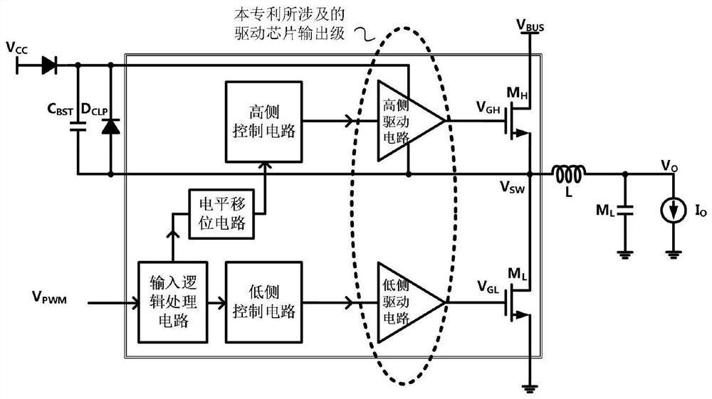
[0027] see figure 1 , which is a functional block diagram of a typical fully integrated driver chip in the prior art. Enhancement Mode GaN FET M H , M L For on-chip integrated GaN power transistors, M H the drain with M L The source of the connection is connected to form a typical half-bridge structure, and the connection point is also used as the output node of the half-bridge structure. V PWM The signal is a pulse modulation signal from a pulse modulator, which is used as the input signal of the driver chip. V PWM After the signal is processed by the input logic processing circuit, level shift circuit, low-side control circuit, high-side control circuit, low-side drive circuit and high-side drive circui...


PUM


Abstract

The invention relates to an output stage circuit based on a gallium nitride process integrated circuit and cascade application thereof, the output stage circuit comprises a bootstrap unit and a totem pole type output unit, the bootstrap unit comprises gallium nitride field effect transistors M1 and M2, gallium nitride resistive devices R1 and R2, a gallium nitride process capacitor C1 and a gallium nitride diode D1; a drain electrode of the M1 is connected with one end of the R1 and one end of the capacitor C1, the other end of the R1 is connected with a power supply VDD, a grid electrode of the M1 is connected with a control signal IN1, source electrodes of the M1 and the M2 are grounded, a grid electrode of the M2 is connected with a control signal IN2, a drain electrode of the M2 is connected with one end of the R2 and serves as an output end of the bootstrap unit to be connected with a grid electrode of the M4 in the totem pole type output unit, and the other end of the R2 is connected with the other end of the capacitor C1 and a negative electrode of the diode D1. The positive electrode of the diode D1 is connected with a power supply VDD. More than one output stage circuit based on a gallium nitride process integrated circuit is cascaded, and the output stage circuit is suitable for the occasion of driving a large-size totem pole type output structure.

Description

technical field [0001] The invention relates to a power integrated circuit and a gate drive circuit, in particular to an output stage circuit based on a gallium nitride process integrated circuit and its cascaded application. Background technique [0002] Gallium nitride material is recognized as the third-generation power semiconductor material, and gallium nitride power devices have the characteristics of high speed, high reliability and low loss. The driving method of traditional GaN power devices is to use silicon-based driver chips to control discrete GaN devices, but the insufficient operating frequency of silicon-based driver chips and the parasitic effects of multi-chip connections limit the high-frequency characteristics and reliability of the system poor. In order to solve the above problems, it is often necessary to reduce the process line width, adopt multi-layer wiring, leadless multi-chip packaging and other technologies, but this inevitably brings about a sig...

Claims


Application Information

Patent Timeline
Patent Type & Authority Applications(China)
IPC IPC(8): H03K19/003H03K17/04H03K17/687H02M1/088H02M3/158
CPCH03K19/00315H03K17/04H03K17/6872H02M1/088H02M3/158H03K19/00323Y02B70/10
Inventor 郑逸飞周琦祝靖张伟陆兆俊施刚吴天阳余思远
Owner 无锡安趋电子有限公司
Learn More