


Quick Research
Generate reliable direction feasibility study reports for your R&D in just a few steps.

Technical Q&A
Discover and master advanced knowledge NOW. Basics, ideas, possibilities, all at once.

Find Solutions
As an expert in R&D theories, this can generate solutions to your technical problems instantly.

Evaluate Feasibility
Analyze your overall solution with one click, know your potential R&D risks in advance.

Monitor Landscape
Get weekly tech updates, stay abreast of the latest tech innovations and key insights.
Optical component and timepiece
一种光学部件、钟表的技术,应用在光学元件、光学、钟表等方向,能够解决无法确保光学部件透过性、无法有效地防止静电污垢的附着等问题,达到优异防反射功能、优异抗静电功能、视觉辨认性优异的效果
- Summary
- Abstract
- Description
- Claims
- Application Information
AI Technical Summary
Problems solved by technology
Method used
Image

Examples
no. 1 Embodiment approach
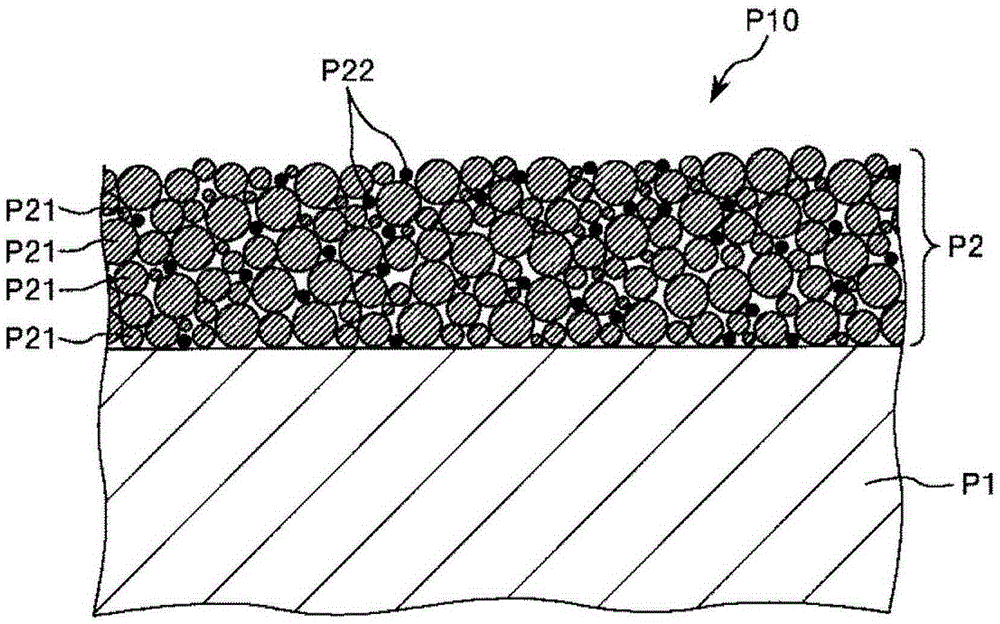
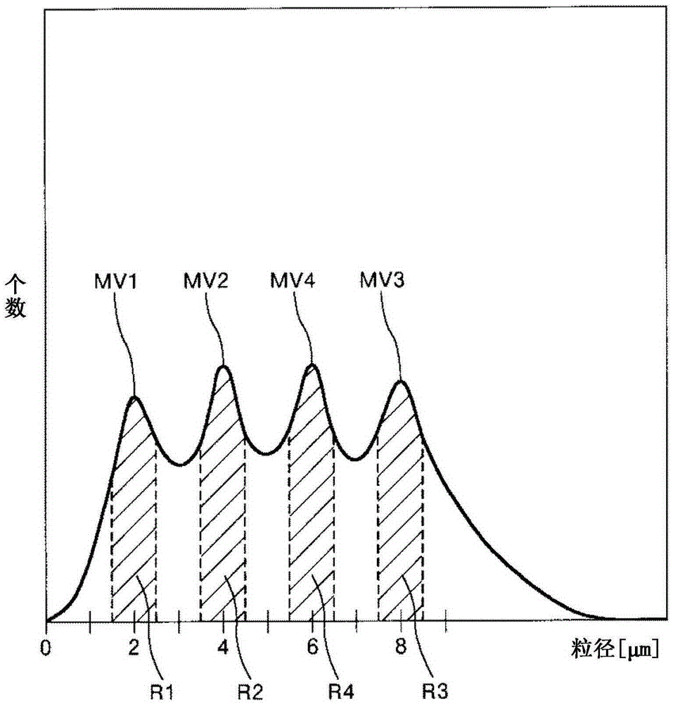
[0042] figure 1 It is a cross-sectional view schematically showing the first embodiment of the optical component of the present invention. figure 2 It is a figure which schematically shows an example of the particle size distribution of the silica particle which comprises the film of the optical component of this invention.
[0043] Such as figure 1 As shown, the optical component P10 of the present embodiment includes: a base material P1; and a film P2 containing silica particles P21 and conductive transparent metal oxide particles P22.
[0044] With such a structure, the antistatic function of the optical component P10 as a whole is exhibited. In other words, the film P2 can function as an antistatic film. As a result, for example, adhesion of dirt such as dust due to static electricity can be prevented, and the optical component P10 can stably exhibit the inherent optical characteristics.
[0045] In addition, since both the silica particles P21 and the conductive tran...
no. 2 Embodiment approach
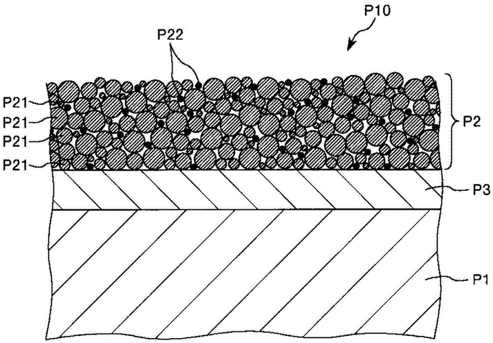
[0127] image 3It is a cross-sectional view schematically showing a second embodiment of the optical component of the present invention. In the following description, differences from the above-described embodiment will be mainly described, and descriptions of the same matters will be omitted.
[0128] Such as image 3 As shown, the optical component P10 of the present embodiment includes: a substrate P1; a film P2 containing silica particles P21 and conductive transparent metal oxide particles P22; and an underlayer P3.
[0129] By having the base layer P3 in this way, for example, the adhesion between the base material P1 and the film P2 (adhesion through the base layer P3) can be particularly excellent, and the durability and reliability of the optical component P10 can be particularly excellent.
[0130] As a constituent material of the base layer P3, for example, various resin materials, SiO 2 Wait.
[0131] The thickness of the base layer P3 is not particularly limit...
Embodiment 1
[0204] A cover glass as an optical component was manufactured by the method shown below.
[0205] First, a plate material (glass plate) made of sapphire glass is prepared as a base material (base material preparation process), and necessary parts are cut and polished. The base material after cutting and grinding was approximately disc-shaped, and had a size of diameter: 30 mm×thickness: 1 mm.
[0206] Next, an ultraviolet irradiation treatment of irradiating ultraviolet rays having a wavelength of 248 nm is performed on the surface of the substrate on which the antireflection film is to be formed.
[0207] Next, the film-forming composition is applied to the entire surface of the substrate by a spraying method (film-forming composition applying step).
[0208] As the film-forming composition, silica particles, tin oxide (SnO 2 ) particles (average particle diameter based on number: 2.0 nm) and methanol as a dispersion medium.
[0209] Silica particles that have the first ma...
PUM
| Property | Measurement | Unit |
|---|---|---|
| particle diameter | aaaaa | aaaaa |
| particle diameter | aaaaa | aaaaa |
| particle diameter | aaaaa | aaaaa |
Abstract
Description
Claims
Application Information
 - R&D Engineer
- R&D Manager
- IP Professional
- Industry Leading Data Capabilities
- Powerful AI technology
- Patent DNA Extraction
Browse by: Latest US Patents, China's latest patents, Technical Efficacy Thesaurus, Application Domain, Technology Topic, Popular Technical Reports.
© 2024 PatSnap. All rights reserved.Legal|Privacy policy|Modern Slavery Act Transparency Statement|Sitemap|About US| Contact US: help@patsnap.com