
Panel compensation device and method

A compensating device and panel technology, applied in the direction of cathode ray tube indicators, instruments, static indicators, etc., can solve the problems of rising manufacturing costs, lower yield rate of liquid crystal panels, uneven brightness of liquid crystal panels, etc., to improve measurement efficiency, The effect of maintaining the accuracy of temperature data

Inactive Publication Date: 2016-06-15
BOE TECH GRP CO LTD +1
View PDF6 Cites 22 Cited by
  • Summary
  • Abstract
  • Description
  • Claims
  • Application Information

AI Technical Summary

Problems solved by technology

The display flaws described above are completely unacceptable to users
[0004] The existence of display defects will reduce the yield of LCD panels
Although the industry has tried to reduce this defect by improving the manufacturing process to improve the yield, this will lead to a significant increase in manufacturing costs
Therefore, how to eliminate or suppress the uneven brightness of LCD panels at low cost has become a thorny problem that plagues the industry.

Method used


Image

  • Panel compensation device and method
  • Panel compensation device and method
  • Panel compensation device and method

Examples


specific Embodiment

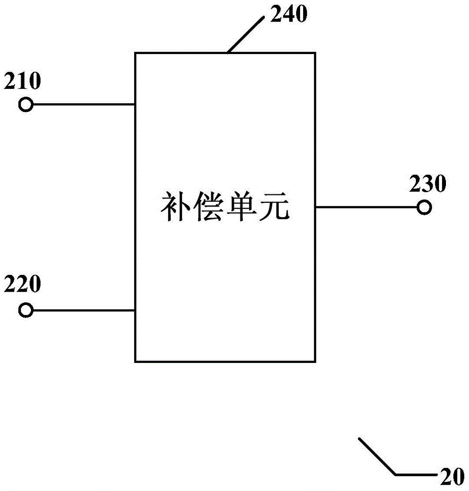
[0059] figure 2 The illustrated device 20 comprises a first input 210 , a second input 220 , an output 230 and a compensation unit 240 , wherein the compensation unit 240 is coupled to the first input 210 , the second input 220 and the output 230 .

[0060] In this embodiment, the first input terminal 210 receives a display driving signal applied to each pixel of the liquid crystal panel, and the second input terminal 220 receives a temperature signal associated with each pixel. As will be further described below, the compensation unit 240 compensates the display driving signals of the pixels in the abnormal display area from the first input terminal 210 based on the reference compensation coefficient and the temperature signal at the same time, so that at the same display driving signal voltage Horizontally, these pixels have the same brightness as pixels in the normal display area. The compensated display driving signal is sent to the liquid crystal panel through the outpu...


PUM


Abstract

The invention relates to the display technology, and more particularly relates to a panel compensation device and a panel compensation method used for eliminating uneven brightness of an LCD panel, and a display device comprising the panel compensation device. The panel compensation device comprises a first input end, a second input end, a compensation unit and an output end, wherein the first input end is configured to receive a display driving signal applied on each pixel; the second input end is configured to receive a temperature signal associated with each pixel; the compensation unit is coupled with the first input end and the second input end, and is configured to compensate for the display driving signals of the pixels in an abnormal display region from the first input end, so that the pixels have identical brightness under the same voltage level of the display driving signals; and the output end is coupled with the compensation unit, and is configured to output the compensated display driving signals.

Description

technical field [0001] The present invention relates to display technology, in particular, to a panel compensation device and method and a display device including the above device. Background technique [0002] In a typical active-matrix liquid crystal display, each pixel has a thin-film transistor (TFT), whose gate is connected to the horizontal scan line, the drain is connected to the vertical data line, and the source is connected to the pixel electrode. When a sufficient positive voltage is applied to a scanning line in the horizontal direction, all the TFTs on the line will be turned on. At this time, the pixel electrode of this line will be connected to the data line in the vertical direction, and the video signal will be written Into the pixel, the effect of controlling the color can be achieved by controlling the different light transmittance of the liquid crystal. [0003] During the manufacturing process of the liquid crystal panel, due to unstable manufacturing ...

Claims


Application Information

Patent Timeline
IPC IPC(8): G09G3/36G09G5/10
CPCG09G3/36G09G5/10G09G3/2007G09G3/3208G09G3/3607G09G2320/0233G09G2320/041G09G2330/10G09G3/3685G09G2310/027
Inventor 胡巍浩郭鲁强孟智明程金辉张超
Owner BOE TECH GRP CO LTD
Features
  • Generate Ideas
  • Intellectual Property
  • Life Sciences
  • Materials
  • Tech Scout
  • Unparalleled Data Quality
  • Higher Quality Content
  • 60% Fewer Hallucinations
Learn More