Method for forming semiconductor structure

A semiconductor and graphics technology, applied in semiconductor/solid-state device manufacturing, electrical components, circuits, etc., can solve the problems of poor resolution of semiconductor graphics and inconsistent shapes of semiconductor graphics, and achieve the effect of improving shape resolution

Active Publication Date: 2016-06-29
SEMICON MFG INT (SHANGHAI) CORP
View PDF2 Cites 18 Cited by
  • Summary
  • Abstract
  • Description
  • Claims
  • Application Information

AI Technical Summary

Problems solved by technology

However, in the existing self-aligned double exposure technology, such as image 3 As shown, after removing the sacrificial pattern 02, the side wall 04 may be inclined towards the original position of the sacrificial pattern 02, or the side wall 04 may also be inclined towa

Method used


Image

  • Method for forming semiconductor structure
  • Method for forming semiconductor structure
  • Method for forming semiconductor structure

Examples


Example Embodiment

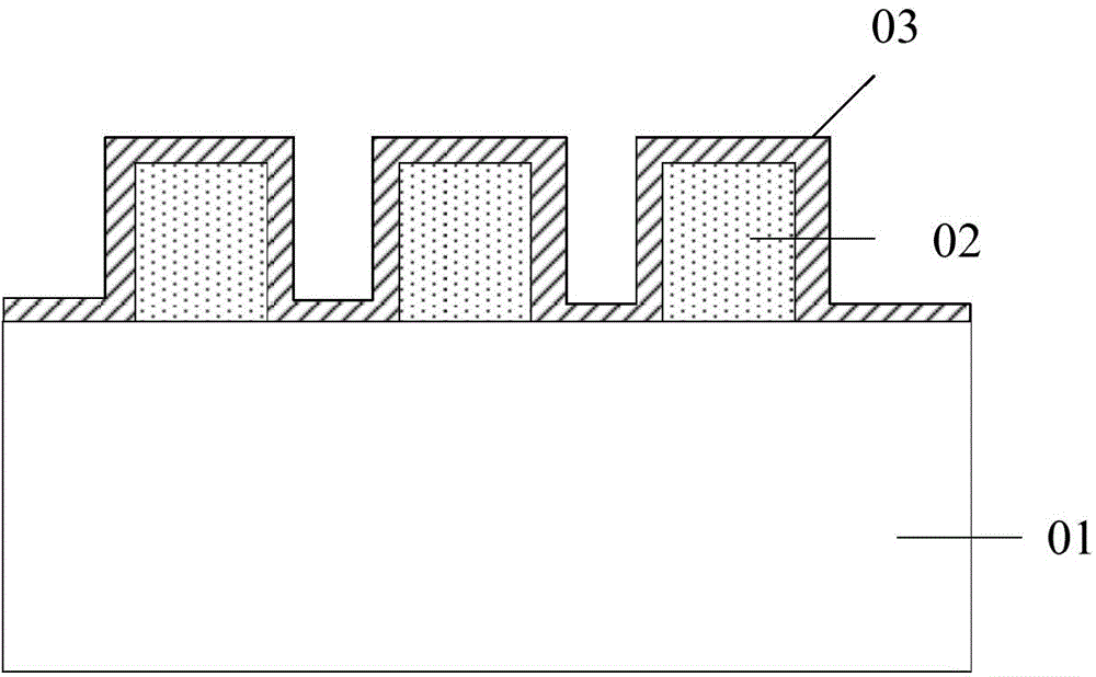
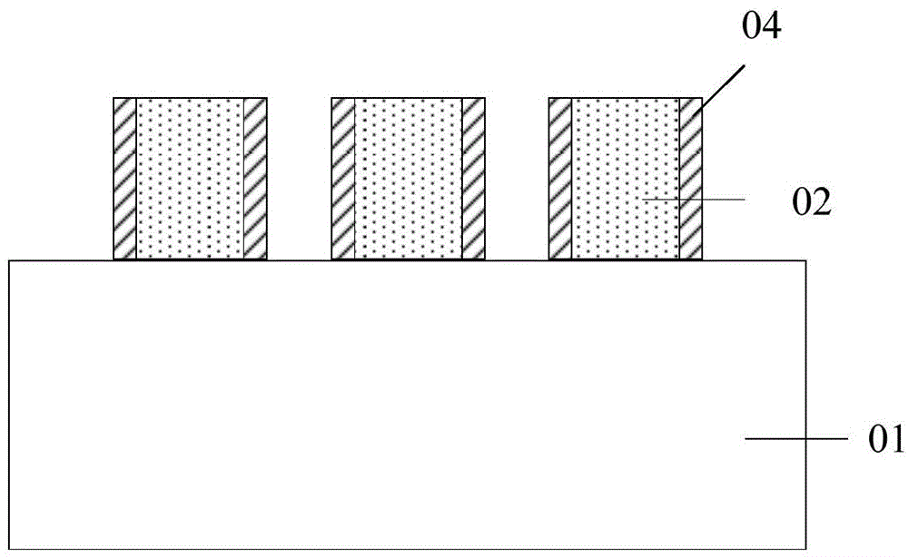
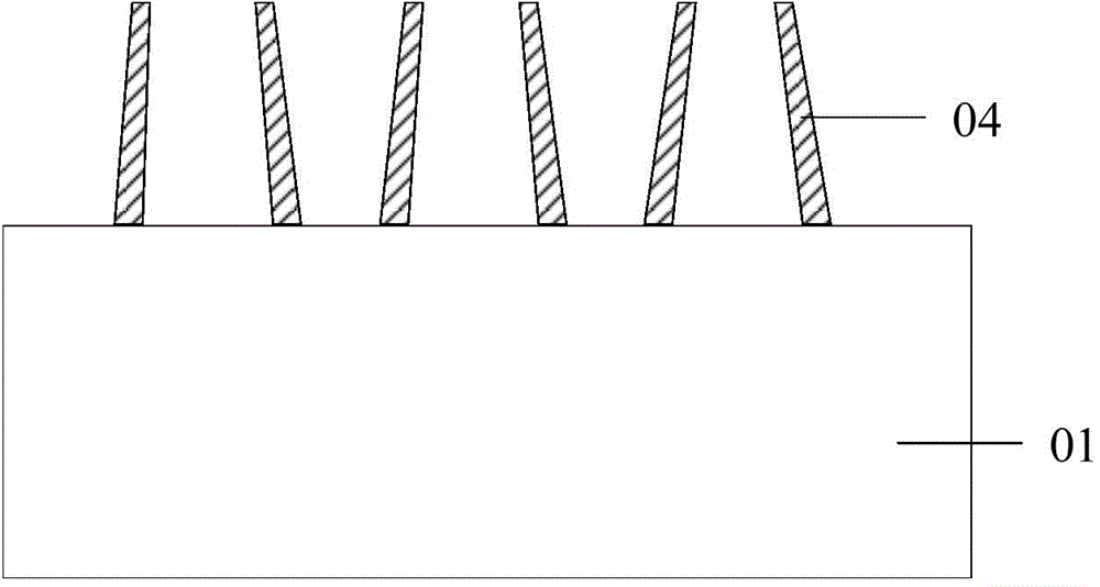
[0032] In the prior art self-aligned double exposure, the sidewalls are prone to tilt due to the effect of stress. Using the inclined sidewalls as a mask to etch the substrate, the formed semiconductor pattern has poor morphology and the shape of the semiconductor pattern It is easy to be distorted compared to the shape to be formed. Analyze the reason why the side wall is prone to tilt: in the step of depositing the side wall material layer, the stress in the side wall material layer is relatively large. After the side wall is formed, the stress inside the side wall is relatively large, and it is located at different positions on the substrate The stress direction of the side wall may be different, which may be tensile stress or compressive stress. After the sacrifice pattern is removed, the side wall may be inclined toward the original position of the sacrifice pattern, or may be inclined to the original position of the sacrifice pattern.

[0033] In order to solve the above te...


PUM


Abstract

The invention provides a method for forming a semiconductor structure, and the method comprises the steps: providing a substrate; forming a sacrifice pattern on the substrate; depositing side wall material layers on the sacrifice pattern and the substrate through employing deposition equipment, carrying out the etching of the side wall material layers, and forming side walls on side walls of the sacrifice pattern; taking the side walls as hard masks, carrying out the etching of the substrate, and forming a semiconductor figure. The deposition equipment is employed for depositing the side wall material layers on the sacrifice pattern and the substrate, and the output radio frequency power of the deposition equipment is switched between the first power and the second power in the deposition process of the side wall material layers, wherein the first power and the second power have different frequencies. The method can enable tension stress and compression stress generated in the side wall material layers to be counteracted with each other partly, thereby enabling the total stress in the side walls to be smaller after the side walls are formed through the etching of the side wall material layers, and enabling the deformation not to be liable to happen. The feature size of the semiconductor figure is smaller when the side walls are taken as the masks.

Description

Technical field [0001] The invention relates to the field of semiconductors, in particular to a method for forming a semiconductor structure. Background technique [0002] As the feature size of the semiconductor photolithography process continues to shrink, it is difficult for the existing exposure equipment to further reduce the minimum line width and spacing of the pattern by reducing the pattern size on the mask. [0003] In order to further reduce the minimum line width and spacing of the graphics, the prior art has developed a self-aligned double exposure (Self-Aligned Double Pattern, SADP) technology. Figure 1 to Figure 3 Shows a part of the common self-aligned double exposure process: the sacrificial pattern 02 is defined by photolithography on the substrate 01, and a thin film 03 is deposited on the top and sidewalls of the substrate 01 and the sacrificial pattern 02 Etch the film 03, remove the film 03 on the substrate 01 and on the top of the sacrificial pattern 02, form...

Claims


Application Information

Patent Timeline
IPC IPC(8): H01L21/027H01L21/033
Inventor 周祖源诸海丰
Owner SEMICON MFG INT (SHANGHAI) CORP
Why Eureka
Try Eureka