
Self-aligned gate contact structure

A gate and contact technology, applied in the field of self-aligned gate contact structure and its formation, can solve the problem of not preventing short circuit of gate contact

Inactive Publication Date: 2016-07-06
GLOBALFOUNDRIES INC
View PDF5 Cites 2 Cited by
  • Summary
  • Abstract
  • Description
  • Claims
  • Application Information

AI Technical Summary

Problems solved by technology

[0005] While the borderless contact process described above prevents shorts between the S / D contacts and the gate, it does not prevent shorts between the gate contacts and the active area of ​​the S / D

Method used


Image

  • Self-aligned gate contact structure
  • Self-aligned gate contact structure
  • Self-aligned gate contact structure

Examples


Embodiment Construction

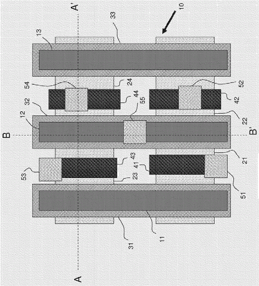
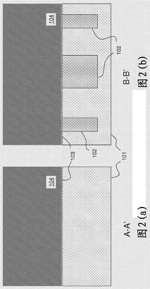
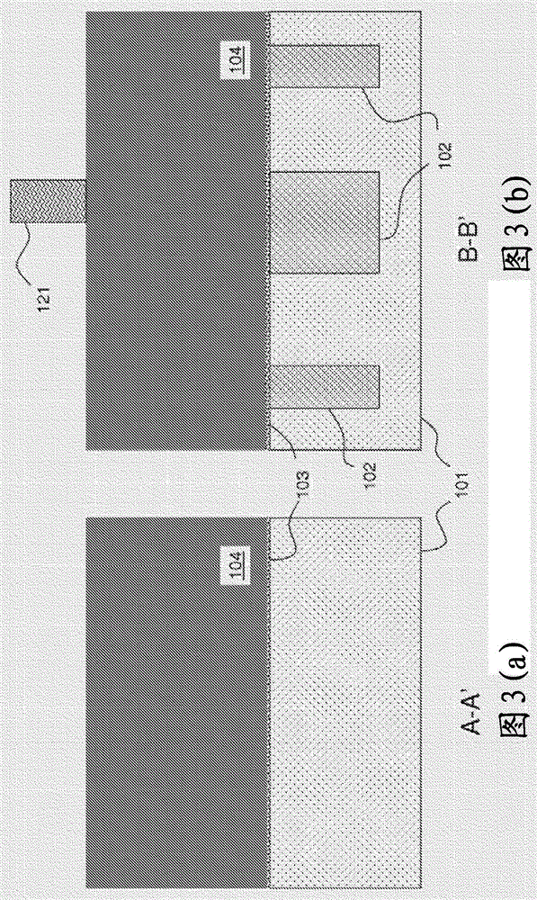
[0024] In the following detailed description, numerous specific details are set forth in order to provide a thorough understanding of various embodiments of the invention. However, it is understood that embodiments of the invention may be practiced without these specific details.

[0025] In order not to obscure the essence of the present invention and / or the expression of the embodiments, in the following detailed description, for expression and / or for illustration, some processing steps and / or operations known in the art may be combined together, and in some instances may not be described in detail. In other instances, some process steps and / or operations known in the art may not be described at all. Additionally, some well-known device processing techniques may not be described in detail, and in some instances other published articles, patents, and / or published patent applications may be referred to by reference so as not to obscure the essence and / or embodiments of the pr...


PUM


Abstract

A method of forming a semiconductor device, the method includes depositing a layer of metal over one or more channel regions of respective one or more transistors in a substrate, the layer of metal having a first region and a second region; lowering height of the first region of the layer of metal; forming an insulating layer over the first region of lowered height, the insulating layer being formed to have a top surface coplanar with the second region of the layer of metal; and forming at least one contact to a source / drain region of the one or more transistors. Structure of the semiconductor device formed thereby is also provided.

Description

technical field [0001] The present invention relates generally to the field of semiconductor device fabrication, and more particularly, to self-aligned gate contact structures and methods of forming the same. Background technique [0002] The continuous scaling down of the fabrication of complementary metal-oxide-semiconductor (CMOS) transistors has currently led to borderless contacts (also known as self-aligned contacts ( SAC)) development. This is primarily because conventional fabrication processes for S / D contacts have frequently been found to cause problems such as electrical shorting between the gate of the transistor and the S / D, where such electrical shorting can sometimes detract from the performance of the transistor. This is especially true in the case of highly shrinking semiconductor device fabrication where the pitch between a transistor and its neighboring transistors can sometimes become extremely narrow or small. In contrast, borderless or self-aligned co...

Claims


Application Information

Patent Timeline
IPC IPC(8): H01L21/28H01L29/423
CPCH01L29/4958H01L29/4966H01L29/78H01L21/823456H01L21/823475H01L21/76897H01L27/088H01L29/66477
Inventor V·巴斯克程慷果A·克哈基弗尔鲁茨V·Y·萨德塞R·斯瑞尼瓦萨恩
Owner GLOBALFOUNDRIES INC
Learn More