Manufacturing method for wavelength conversion device

A technology of wavelength conversion device and wavelength conversion layer, which is applied to components of lighting devices, lighting devices, lighting and heating equipment, etc., can solve problems such as high equipment requirements, complicated procedures, and unsuitable production, so as to prevent adverse effects and improve Reliability, the effect of reducing the time at high temperature

Active Publication Date: 2016-07-27
APPOTRONICS CORP LTD
View PDF4 Cites 26 Cited by
  • Summary
  • Abstract
  • Description
  • Claims
  • Application Information

AI Technical Summary

Problems solved by technology

[0005] However, the above-mentioned first preparation method has complex procedures and high equipment requirements, and is not suitable for production
In the second preparation method, the entire wavelength conversion device needs to be placed in a high-temperature furnace. In order to ensure the sintering density, the sintering temperature is generally required to be above 400°C. The silver-coated layer will generally have sulfuration and oxidation at a high temperature of 400°C. Reduced reliability of switching devices

Method used


Image

  • Manufacturing method for wavelength conversion device
  • Manufacturing method for wavelength conversion device

Examples


preparation example Construction

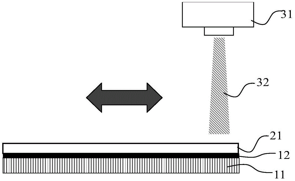
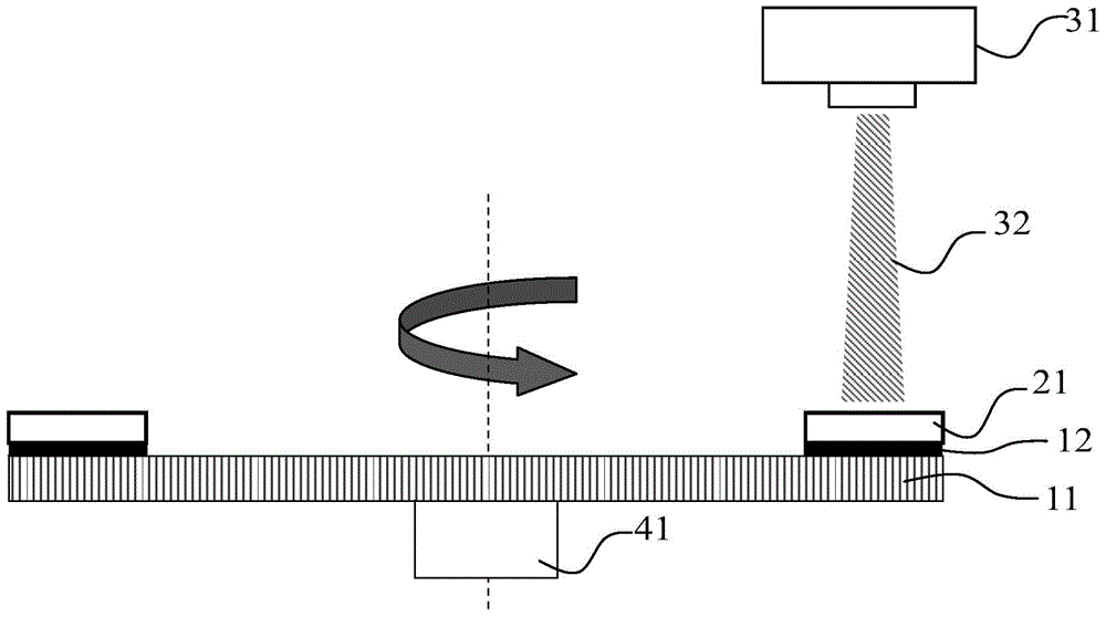
[0024] As mentioned in the background technology section, the manufacturing method of the wavelength conversion device in the prior art has the defect that the reflective layer of the wavelength conversion device cannot withstand high temperature, resulting in low reliability of the wavelength conversion device. In order to improve the above situation, the present invention provides A method for preparing a wavelength conversion device, the preparation method comprising the following steps: providing a thermally conductive substrate prepared with a reflective layer; mixing phosphor powder and a transparent inorganic adhesive to form a slurry; coating the slurry on the reflective layer of the thermally conductive substrate above, forming a wavelength conversion layer green sheet; using a laser to sinter the wavelength conversion layer green sheet to obtain a wavelength conversion device.

[0025] In the above-mentioned preparation method of the present invention, the mixed slurr...


PUM

PropertyMeasurementUnit
softening pointaaaaaaaaaa
transmittivityaaaaaaaaaa

Abstract

The invention discloses a manufacturing method for a wavelength conversion device. The manufacturing method includes the following steps that a heat conduction substrate on which a reflecting layer is manufactured is provided; fluorescent powder and a transparent inorganic bonding agent are mixed to form slurry; the reflecting layer of the heat conduction substrate is coated with the slurry, and a wavelength conversion laminated sheet is formed; and lasers are used for sintering the wavelength conversion laminated sheet, and the wavelength conversion device is obtained. By means of the above manufacturing method, the heat conduction substrate with the reflecting layer is coated with the slurry formed by mixing the transparent inorganic bonding agent and the fluorescent powder, sintering is conducted in a laser illumination manner so that the lasers can penetrate the transparent inorganic bonding agent to form light-emitting heat sources at the positions of all fluorescent powder particles, and therefore an overall fluorescent material layer is rapidly heated at the same time; and meanwhile, the heat conduction substrate with the reflecting layer can transmit heat generated by the fluorescent material layer out rapidly to lower the temperature of the reflecting layer, and therefore the reliability of the manufactured wavelength conversion device is improved.

Description

technical field [0001] The invention relates to the field of photoelectric conversion technology, in particular to a method for preparing a wavelength conversion device. Background technique [0002] With the development of display and lighting technology, the original LED or halogen bulb as a light source is increasingly unable to meet the high power and high brightness requirements of display and lighting. Visible light of various colors can be obtained by using excitation light emitted by a solid-state light source such as LD (Laser Diode, laser diode) to excite wavelength conversion materials, and this technology is increasingly used in lighting and display. This technology has the advantages of high efficiency, low energy consumption, low cost, and long life, and is an ideal alternative to existing white or monochromatic light sources. [0003] In the prior art, in order to improve the light utilization rate, the light sources of laser-excited wavelength-converting mat...

Claims


Application Information

Patent Timeline
Patent Type & Authority Applications(China)
IPC IPC(8): F21V9/10F21V9/40
Inventor 田梓峰李乾徐虎
Owner APPOTRONICS CORP LTD
Why Eureka
Try Eureka