A device for disassembling a dual in-line package chip

A dual-in-line packaging and disassembly device technology, which is applied in metal processing equipment, welding equipment, manufacturing tools, etc., can solve the problems of complicated operation process, damage, and difficult maintenance operation, and achieve the effect of reducing the heating area and preventing damage

Active Publication Date: 2019-05-07
ARMY ENG UNIV OF PLA
View PDF8 Cites 0 Cited by
  • Summary
  • Abstract
  • Description
  • Claims
  • Application Information

AI Technical Summary

Problems solved by technology

One method is to manually disassemble with an electric soldering iron. It is difficult to melt the solder on all pins at the same time and take out the chip. It usually needs to be repeated many times to remove some pins in stages, which will easily cause deformation of the circuit board and solder joints. fall off, making subsequent maintenance operations very difficult
Another common method is to use a tin furnace. The heating surface of the tin furnace is large, and all the pins of the chip can be melted and removed at the same time. However, large-area heating can easily cause damage to the chip to be disassembled due to excessive heat, and it is easy to treat. Demolition of components and circuit boards around the chip causes irreparable damage
This process not only needs to fix the circuit board to be repaired, but also needs to operate the electric soldering iron, and use the chip puller to remove the chip to be removed. The operation process is very complicated, and the connection should be very tight to disassemble successfully.

Method used


Image

  • A device for disassembling a dual in-line package chip
  • A device for disassembling a dual in-line package chip
  • A device for disassembling a dual in-line package chip

Examples


Embodiment Construction

[0014] The present invention is described in further detail below by embodiment.

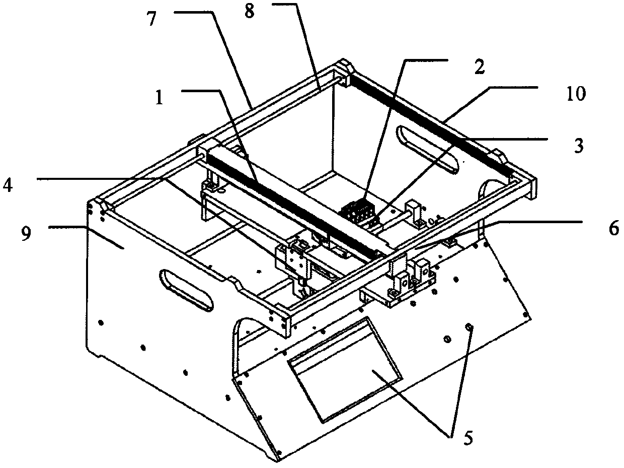
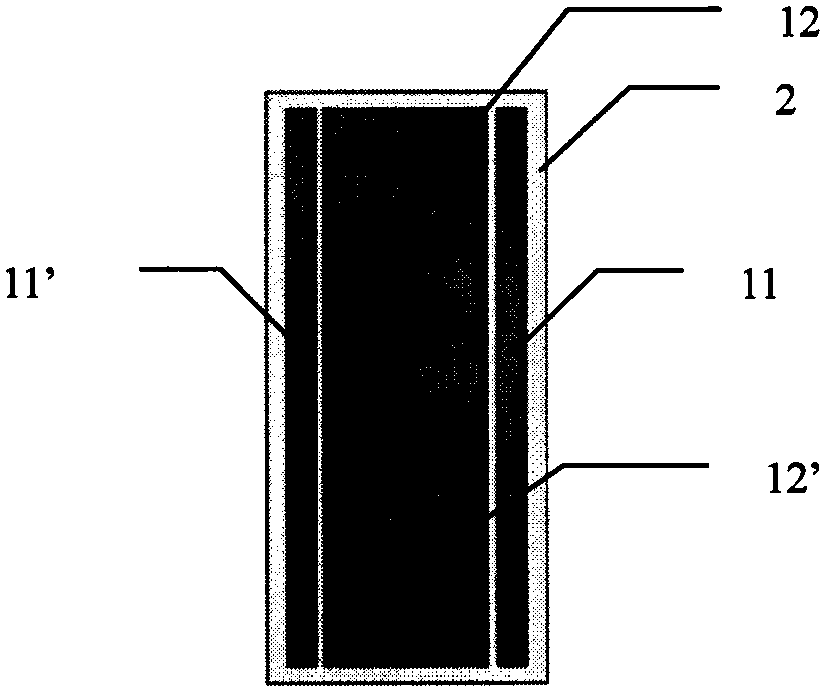
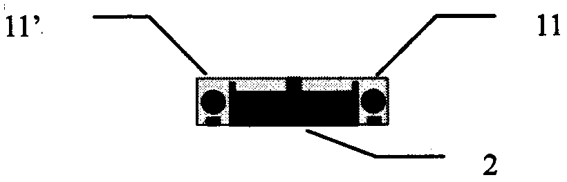
[0015] The schematic diagram of the structure of the dual in-line package chip removal device (hereinafter referred to as the removal device) is as follows figure 1 As shown, it includes a circuit board fixing unit 1, a tin bath unit 2, a heating temperature control unit 3, a positioning unit 4, an operation display unit 5 and frames 6, 7, 9, 10.

[0016] Wherein, the circuit board fixing unit 1 is positioned at the top of the dismounting device, one end of which is vertically connected to the front frame 6 of the dismounting device, and the other end is vertically connected to the cylindrical cross bar 8 on the rear frame 7 which is horizontal to the front frame 6, along the The circuit board fixing unit 1 can be pushed along the vertical direction of the circuit board fixing unit 1 . There are three grooves matching the thickness of the circuit board on the left and right sides of the circuit...


PUM


Abstract

The invention relates to a dual-in-line package chip dismounting device which can solve the problem that a dual-in-line package chip is difficult to dismount rapidly in a lossless manner during maintenance of a circuit board. The dual-in-line package chip dismounting device includes a circuit board fixing unit (1), a molten tin bath unit (2), a heating temperature-control unit (3), a positioning unit (4), an operation display unit (5) and frames (6, 7, 9, 10). The dual-in-line package chip dismounting device is easy to operate, can rapidly dismount dual-in-line package chips with different pins from the circuit board in a lossless manner.

Description

technical field [0001] The invention relates to a device that can be used to remove a dual in-line package chip from a circuit board. Background technique [0002] With the rapid development of microelectronics technology, there are many applications and types of dual in-line package chips in modern weaponry. When a chip is damaged, it needs to be removed from the circuit board for testing or replacement for repair. Dual-in-line package chips usually have many pins and a large span. When disassembling, it is usually necessary to heat and melt the solder of all pins on the chip at the same time. At present, there is no suitable tool device. One method is to manually disassemble with an electric soldering iron. It is difficult to melt the solder on all pins at the same time and take out the chip. It usually needs to be repeated many times to remove some pins in stages, which will easily cause deformation of the circuit board and solder joints. fall off, making subsequent mai...

Claims


Application Information

Patent Timeline
Patent Type & Authority Patents(China)
IPC IPC(8): B23K1/018
Inventor 杨青王春平贺治华王少华朱翔宇王志强付强娄亮李军孙书鹰
Owner ARMY ENG UNIV OF PLA
Why Eureka
Try Eureka