Display panel, manufacturing method and electronic device

A technology for display panels and substrates, which is applied to circuits, electrical components, electrical solid-state devices, etc., can solve problems affecting the image display effect of OLED display panels, and achieve good image display effects.

Active Publication Date: 2019-08-02
WUHAN TIANMA MICRO ELECTRONICS CO LTD +1
View PDF4 Cites 0 Cited by
  • Summary
  • Abstract
  • Description
  • Claims
  • Application Information

AI Technical Summary

Problems solved by technology

If leakage occurs, it will affect the image display effect of the OLED display panel

Method used


Image

  • Display panel, manufacturing method and electronic device
  • Display panel, manufacturing method and electronic device
  • Display panel, manufacturing method and electronic device

Examples


Embodiment Construction

[0035] The following will clearly and completely describe the technical solutions in the embodiments of the present invention with reference to the accompanying drawings in the embodiments of the present invention. Obviously, the described embodiments are only some, not all, embodiments of the present invention. Based on the embodiments of the present invention, all other embodiments obtained by persons of ordinary skill in the art without making creative efforts belong to the protection scope of the present invention.

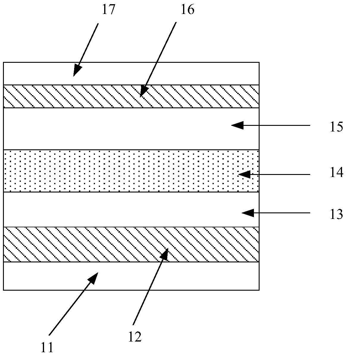
[0036] The structure of the existing OLED display panel is as follows figure 1 as shown, figure 1 It is a schematic structural diagram of a common OLED display panel in the prior art. figure 1 From bottom to top, the OLED display panel includes a substrate 11 , an anode layer 12 , a first common layer 13 , a light emitting layer 14 , a second common layer 15 , a cathode layer 16 and a cover plate 17 arranged in sequence. The OLED display panel has a pluralit...


PUM


Abstract

The invention discloses a display panel, a manufacturing method and electronic equipment. The display panel comprises: a substrate; an anode layer and a pixel definition layer located on the same side of the substrate; the anode layer includes a plurality of anodes arranged in an array, and the anode includes a first electrode Part; the pixel definition layer includes a plurality of pixel openings, the pixel openings correspond to the anodes one by one, and the pixel openings are used to expose the first electrode part; the first common layer located on the side of the pixel definition layer and the anode away from the substrate; the first common layer includes At least one preset sub-functional layer; the preset sub-functional layer has a partition structure; a light-emitting layer arranged on the surface of the first common layer; the light-emitting layer includes a plurality of light-emitting units corresponding to the pixel openings; the light-emitting units are located in the pixel openings , and completely cover the first electrode part; the cathode layer located on the side of the light-emitting layer away from the substrate. The display panel can prevent leakage current through the isolation structure.

Description

technical field [0001] The present invention relates to the technical field of display devices, and more specifically, to a display panel, a manufacturing method and electronic equipment. Background technique [0002] In recent years, flat panel displays such as LCD displays and OLED displays have gradually replaced CRT displays and become mainstream products in the display market. Among them, OLED displays have many advantages such as self-illumination, low driving voltage, high luminous efficiency, short response time, high definition and contrast, wide viewing angle range, wide operating temperature range, flexible display and large-area full-color display. It is considered by the industry to be the display with the most development potential. [0003] The main structure of the OLED display device is an OLED display panel, and the OLED display panel includes an anode and a cathode arranged oppositely; and a functional layer arranged between the anode and the cathode. Th...

Claims


Application Information

Patent Timeline
Patent Type & Authority Patents(China)
IPC IPC(8): H01L27/32
CPCH10K59/12H10K59/1201
Inventor 范刘静韩立静
Owner WUHAN TIANMA MICRO ELECTRONICS CO LTD
Why Eureka
Try Eureka