Pixel circuit and driving method thereof, array substrate, display panel and display device

A technology of a pixel circuit and a driving method, which is applied in the display field, can solve problems such as increased power consumption, achieve the effects of increasing substrate space, ensuring image display effects, and avoiding power consumption

Active Publication Date: 2020-02-21
BOE TECH GRP CO LTD
View PDF10 Cites 0 Cited by
  • Summary
  • Abstract
  • Description
  • Claims
  • Application Information

AI Technical Summary

Problems solved by technology

[0003] Among them, unlike TFT-LCD which uses a stable voltage to control brightness, OLED is current-driven and requires a stable current to control light emission; in the most primitive 2T1C pixel circuit (such as figure 1 ), when displaying a static image, the switching transistor needs to be continuously refreshed, and the switching transistor will generate a certain amount of power consumption during the refreshing process, thereby increasing the power consumption

Method used


Image

  • Pixel circuit and driving method thereof, array substrate, display panel and display device
  • Pixel circuit and driving method thereof, array substrate, display panel and display device
  • Pixel circuit and driving method thereof, array substrate, display panel and display device

Examples


Embodiment Construction

[0032] The present invention will be further described below with reference to the accompanying drawings and exemplary embodiments, wherein the same reference numerals in the accompanying drawings all refer to the same components. Also, detailed descriptions of known arts will be omitted if they are unnecessary to illustrate the features of the present invention.

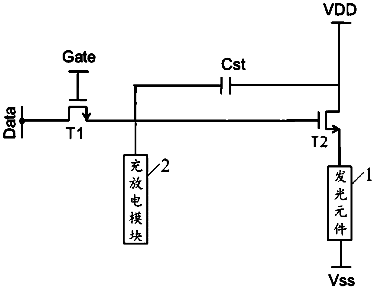
[0033] A schematic structural diagram of a typical embodiment of a pixel circuit provided by the present invention is shown in Figure 2. The pixel circuit includes a switching transistor T1, a storage capacitor Cst, a driving transistor T2, a light-emitting element 1, and a drain of the switching transistor T1. A charging and discharging module 2 that is connected to poles and can control the charging and discharging state in real time.

[0034] Wherein, the source of the switching transistor T1 is externally connected to the data signal terminal Data, the gate of the switching transistor T1 is externally connected ...


PUM


Abstract

The present invention relates to the field of display technology, in particular to a pixel circuit and a driving method thereof, an array substrate, a display panel and a display device. The pixel circuit includes a switch transistor, a storage capacitor, a drive transistor, and a light-emitting element, and also includes a charge and discharge module connected to the drain of the switch transistor and capable of real-time control of the charge and discharge state; when the switch transistor is turned on to conduct current The charging and discharging module implements charging, and when the switching transistor is turned off and the storage capacitor is insufficient, the charging and discharging module implements discharging to supply power to the light-emitting element. Therefore, the present invention not only does not need to perform threshold voltage compensation, but reduces the substrate space occupied by the threshold voltage compensation circuit, so as to make full use of the substrate space to increase the pixel density, and can avoid more power consumption due to frequent refreshing of switching transistors, so as to greatly reduce Power consumption; at the same time, it can intelligently control different duty cycles and time allocation, thereby realizing multi-gray scale display.

Description

【Technical field】 [0001] The present invention relates to the field of display technology, in particular to a pixel circuit and a driving method thereof, an array substrate, a display panel and a display device. 【Background technique】 [0002] Organic light-emitting display (Active Matrix Organic Light Emitting Diode, referred to as AMOLED) is one of the hot spots in the field of flat panel display research today. Compared with liquid crystal displays, OLED has low energy consumption, low production cost, self-illumination, wide viewing angle and fast response speed, etc. Advantages, at present, OLED has begun to replace traditional LCD display screens in display fields such as mobile phones, PDAs, and digital cameras. Pixel drive circuit design is the core technical content of AMOLED display, which has important research significance. [0003] Among them, unlike TFT-LCD which uses a stable voltage to control brightness, OLED is current-driven and requires a stable current ...

Claims


Application Information

Patent Timeline
Patent Type & Authority Patents(China)
IPC IPC(8): G09G3/3233
CPCG09G3/3233G09G3/2022G09G2300/0814G09G2300/0819G09G2300/0852G09G3/3258G09G3/3266G09G3/3291G09G2300/0426
Inventor 肖丽陈小川玄明花杨盛际付杰王磊刘冬妮卢鹏程岳晗
Owner BOE TECH GRP CO LTD
Why Eureka
Try Eureka