Electrostatic discharge device and manufacturing method thereof, array substrate, display panel and device

A manufacturing method and discharger technology, which can be applied in the manufacture of semiconductor/solid-state devices, electric solid-state devices, capacitors, etc., and can solve problems such as large space area and so on.

Active Publication Date: 2016-10-12
BOE TECH GRP CO LTD
View PDF8 Cites 5 Cited by
  • Summary
  • Abstract
  • Description
  • Claims
  • Application Information

AI Technical Summary

Problems solved by technology

However, the space occupied by the electrostatic discharge device in the prior art is large and the electrostatic discharge capacity needs to be further improved

Method used


Image

  • Electrostatic discharge device and manufacturing method thereof, array substrate, display panel and device
  • Electrostatic discharge device and manufacturing method thereof, array substrate, display panel and device
  • Electrostatic discharge device and manufacturing method thereof, array substrate, display panel and device

Examples


Embodiment Construction

[0043] In order to make the purpose, technical solutions and advantages of the embodiments of the present invention clearer, the technical solutions of the embodiments of the present invention will be clearly and completely described below in conjunction with the accompanying drawings. Apparently, the described embodiments are some, not all, embodiments of the present invention. Based on the described embodiments of the present invention, all other embodiments obtained by those skilled in the art without creative efforts also fall within the protection scope of the present invention.

[0044] When introducing elements of the invention and embodiments thereof, the articles "a," "an," "the," and "said" are intended to mean that there are one or more of the elements. The terms "comprising," "including," "containing," and "having" are intended to be inclusive and mean that there may be additional elements other than the listed elements.

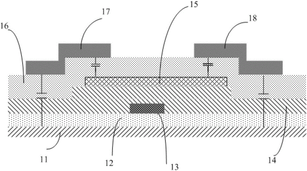
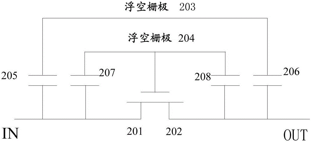
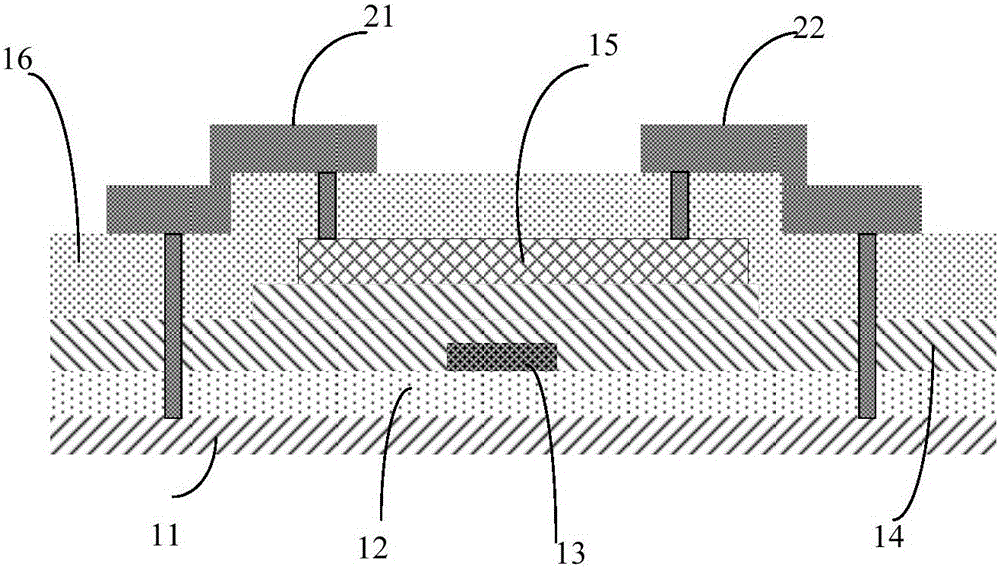
[0045] For purposes of the surface descri...


PUM


Abstract

The invention provides an electrostatic discharge device, a manufacturing method thereof, an active array substrate, a display panel and a display device. The electrostatic discharge device comprises a transistor, wherein one of a source and a drain of the transistor serves as an input end of the electrostatic discharge device, the other serves as an output end; the transistor comprises a first conductive layer serving as a first floating gate, a first insulating layer covering the first conductive layer, an active layer arranged on the first insulating layer, a second insulating layer covering the active layer, a second conductive layer serving as a second floating gate and arranged on the second insulating layer, a third insulating layer covering the second conductive layer, and a third conductive layer and a fourth conductive layer which are arranged on the third insulating layer and separately positioned on two sides of the active layer in a mutual isolated manner; and the third conductive layer serves as one of the source and the drain, and the fourth conductive layer serves as the other.

Description

technical field [0001] The present invention relates to electrostatic discharge (ESD) protection. Specifically, it relates to an electrostatic discharge device, a manufacturing method thereof, an active array substrate, a display panel, and a display device. Background technique [0002] In a display device, in order to prevent damage to a display panel or the like due to static electricity, an electrostatic discharge device is generally provided on the display panel or the like. [0003] As the resolution of the product continues to increase, the pixel design of the product becomes smaller and smaller, which leads to a smaller and smaller space for the ESD design unit around the display area. However, the ESD devices in the prior art occupy a large space and the ESD capability needs to be further improved. Contents of the invention [0004] Embodiments of the present invention provide an electrostatic discharge device, a manufacturing method thereof, an active matrix su...

Claims


Application Information

Patent Timeline
Patent Type & Authority Applications(China)
IPC IPC(8): H01L27/02H01L21/77
CPCH01L27/0266G02F1/136204H01L21/76877H01L21/77H01L27/02H01L27/0288H01L27/1255H01L28/40H01L29/66484H01L29/78648H01L29/788
Inventor 盖翠丽王龙彦王玲李全虎林奕呈
Owner BOE TECH GRP CO LTD
Why Eureka
Try Eureka