Radio frequency PCB connecting structure and connecting method

A connection structure and connection method technology, which is applied in the directions of electrical connection of printed components, formation of electrical connection of printed components, and printed circuit manufacturing, etc., can solve the problem that it is difficult to meet the requirements of RF PCB connection impedance control, and cannot achieve low-cost RF PCB connections. The requirements of the radio frequency signal of the radio frequency board, etc., achieve the effect of easy implementation, good impedance control and grounding, and simple structure

Active Publication Date: 2016-12-07
COMBA TELECOM SYST CHINA LTD
View PDF6 Cites 10 Cited by
  • Summary
  • Abstract
  • Description
  • Claims
  • Application Information

AI Technical Summary

Problems solved by technology

[0003] At present, the existing PCB connection methods mainly fall into the following categories: 1. The contact connection between exposed copper and conductive shrapnel is used between the PCB boards, which is difficult to meet the impedance control requirements in the RF PCB connection; 2. The PCB boards are connected using The connector is used for the connection of the digital board and the transmission of the digital signal, and the cost is low, but it cannot meet the requirements of the RF signal of the RF board, and cannot achieve 50ohm impedance control; 3. Use RF connectors and coaxial cables To connect the RF PCB, this method can obtain good impedance control, but the cost is high, and it will introduce cable loss; 4. The use of RF blind mating connectors is to realize the face-to-face connection of two RF PCB boards, which can also be realized Good performance and space saving, but very expensive
From the above, it can be seen that the existing technology has not been able to realize the RF PCB connection with low cost and good impedance control

Method used


Image

  • Radio frequency PCB connecting structure and connecting method
  • Radio frequency PCB connecting structure and connecting method
  • Radio frequency PCB connecting structure and connecting method

Examples


Embodiment Construction

[0036] In order to make the object, technical solution and advantages of the present invention clearer, the present invention will be further described in detail below in conjunction with the accompanying drawings and specific implementation methods. It should be understood that the specific embodiments described here are only used to explain the present invention, and do not limit the protection scope of the present invention.

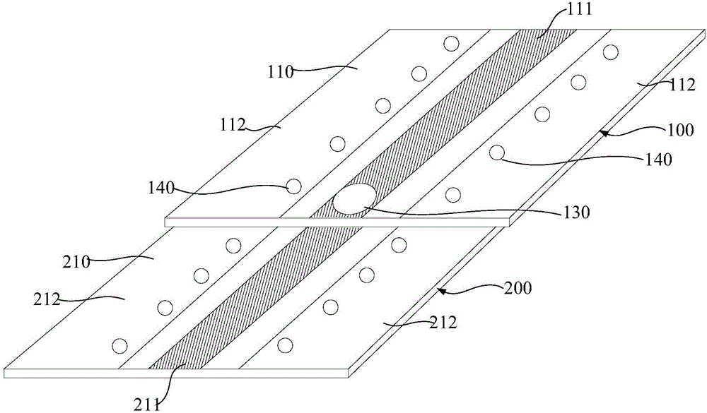
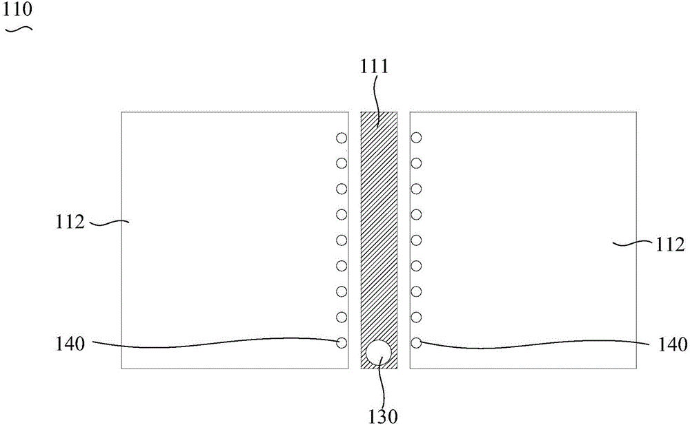
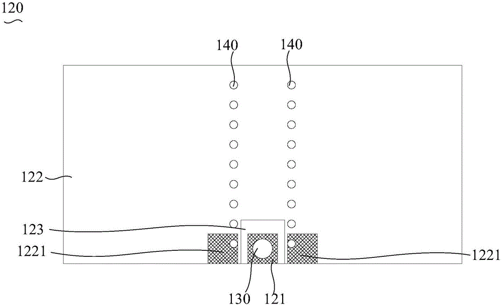
[0037] Such as Figure 1 to Figure 4 As shown, the RF PCB connection structure of the present invention includes a first PCB board 100 and a second PCB board 200, the first PCB board 100 is arranged above the second PCB board 200, and the first PCB board The bottom layer 120 of the board 100 is connected to the top layer 210 of the second PCB board 200 . The top layer 110 of the first PCB board 100 is provided with a first radio frequency circuit 111, the bottom layer 120 of the first PCB board 100 is provided with a first signal pad 121, and the fir...


PUM


Abstract

The invention discloses a radio frequency PCB connecting structure and connecting method. The radio frequency PCB connecting structure comprises a first PCB and a second PCB. The first PCB is arranged above the second PCB, a first radio-frequency circuit is arranged on the top layer of the first PCB, a first signal welding disc is arranged on the bottom layer of the first PCB, and the first radio-frequency circuit is electrically connected with the first signal welding disc through a signal through hole; a second radio-frequency circuit is arranged on the top layer of the second PCB, a second signal welding disc corresponding to the first signal welding disc is arranged on the second radio-frequency circuit, and the first signal welding disc and the second signal welding disc are welded. According to the radio frequency PCB connecting structure and connecting method, the first radio-frequency circuit is communicated with the first signal welding disc through the signal through hole, then the first signal welding disc and the second signal welding disc located on the second radio-frequency circuit are welded, and signal communication between the first radio-frequency circuit and the second radio-frequency circuit is achieved.

Description

technical field [0001] The invention relates to the technical field of PCB connection, in particular to a radio frequency PCB connection structure and a connection method. Background technique [0002] With the rapid development of mobile communication, especially the development of 4G communication, there are more and more demands for product serialization and platformization. In serialized products, modularizing circuits with the same function will effectively reduce the development cycle and reduce the cost. This design concept is also applicable to radio frequency circuits. The use of sub-board design for radio frequency circuits will be more conducive to reducing costs, obtaining better performance, and serialization and platformization. However, how to connect two RF PCBs (Printed Circuit Boards, printed circuit boards) to achieve good RF impedance control and lower cost is the key to serialization, modularization and platformization of RF circuits. [0003] At prese...

Claims


Application Information

Patent Timeline
Patent Type & Authority Applications(China)
IPC IPC(8): H05K1/11H05K3/40
CPCH05K1/11H05K3/4007H05K2201/041
Inventor 范莉张志梅朱艳涛罗成庆
Owner COMBA TELECOM SYST CHINA LTD
Why Eureka
Try Eureka