Shifting register unit, grid driving circuit and organic organic electroluminescence display panel
A shift register, light-emitting signal technology, applied in static memory, digital memory information, instruments, etc., can solve the problems of complex circuit design, large space occupation, and unfavorable OLED display panel narrow frame design.
- Summary
- Abstract
- Description
- Claims
- Application Information
AI Technical Summary
Problems solved by technology
Method used
Image

Examples
no. 1 approach
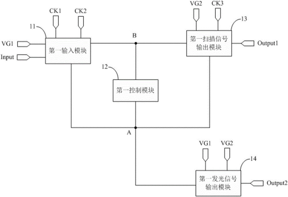
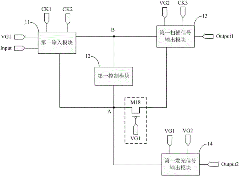
[0085] An embodiment of the present invention provides a shift register unit, such as Figure 1a As shown, it includes: a first input module 11, a first control module 12, a first scan signal output module 13 and a first light emitting signal output module 14; wherein,
[0086] The first terminal of the first input module 11 is connected to the input signal terminal Input, the second terminal is connected to the first clock signal terminal CK1, the third terminal is connected to the second clock signal terminal CK2, and the fourth terminal is connected to the first reference signal terminal VG1 The fifth terminal is connected to the first node A, and the sixth terminal is connected to the second node B; the first input module 11 is used to provide the signal of the input signal terminal Input to the second terminal under the control of the first clock signal terminal CK1 A node A, under the control of the second clock signal terminal CK2, provides the signal of the first refere...
Embodiment 1
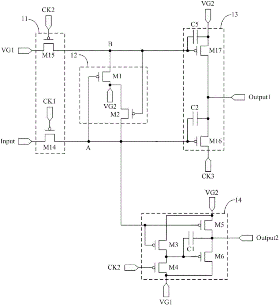
[0143] Such as Figure 3a As shown, all switching transistors in the shift register unit are P-type transistors; VG1=0, VG2=1; the first clock signal terminal CK1 and the second clock signal terminal CK2 are independent of each other; the corresponding input and output timing diagrams are shown in Figure 6a As shown, specifically, the main selection such as Figure 6a The three stages of T1, T2 and T3 in the input and output timing diagram shown.
[0144] In the T1 stage, Input=0, CK1=0, CK2=1, CK3=1.
[0145] Since CK1=0, the fourteenth switch transistor M14 is turned on and provides the signal of the low potential input signal terminal Input to the first node A, so the potential of the first node A is low potential. Since CK2=1, both the fourth switch transistor M4 and the fifteenth switch transistor M15 are turned off. Since the potential of the first node A is low, the first switch transistor M1 , the third switch transistor M3 and the fifth switch transistor M5 are al...
Embodiment 2
[0156] Such as Figure 3c As shown, all the switching transistors in the shift register unit are P-type transistors; the first clock signal terminal CK1 and the second clock signal terminal CK2 are the same signal terminal; VG1=0, VG2=1; the corresponding input and output timing diagram is as follows Figure 6b As shown, specifically, the main selection such as Figure 6b The three stages of T1, T2 and T3 in the input and output timing diagram shown.
[0157] In the T1 stage, Input=0, CK1=0, CK3=1.
[0158] Since CK1=0, both the fourteenth switch transistor M14 and the fifteenth switch transistor M15 are turned on. Since the fourteenth switch transistor M14 is turned on and provides the signal of the low-potential input signal terminal Input to the first node A, the potential of the first node A is low, and the ninth switch transistor M9 and the twelfth switch transistor M12 are both turned on, and the thirteenth switching transistor M13 is turned off. Since VG1=0, the eig...
PUM
 Abstract
Description
Claims
Application Information
 - R&D Engineer
- R&D Manager
- IP Professional
- Industry Leading Data Capabilities
- Powerful AI technology
- Patent DNA Extraction
Browse by: Latest US Patents, China's latest patents, Technical Efficacy Thesaurus, Application Domain, Technology Topic.
© 2024 PatSnap. All rights reserved.Legal|Privacy policy|Modern Slavery Act Transparency Statement|Sitemap