A kind of coptx nanocomposite structure electromagnetic storage device and preparation method

A storage device and nano-composite technology, applied in static memory, electric solid-state devices, digital memory information, etc., to achieve excellent storage performance, conformality and controllability guarantee, and excellent resistive storage function

Active Publication Date: 2019-05-03
NANJING UNIV
View PDF13 Cites 0 Cited by
  • Summary
  • Abstract
  • Description
  • Claims
  • Application Information

AI Technical Summary

Problems solved by technology

The direct application of ALD deposition technology to the preparation of ultra-high-density FePt / CoPt nano-arrays is still blank

Method used


Image

  • A kind of coptx nanocomposite structure electromagnetic storage device and preparation method
  • A kind of coptx nanocomposite structure electromagnetic storage device and preparation method
  • A kind of coptx nanocomposite structure electromagnetic storage device and preparation method

Examples


Embodiment 1

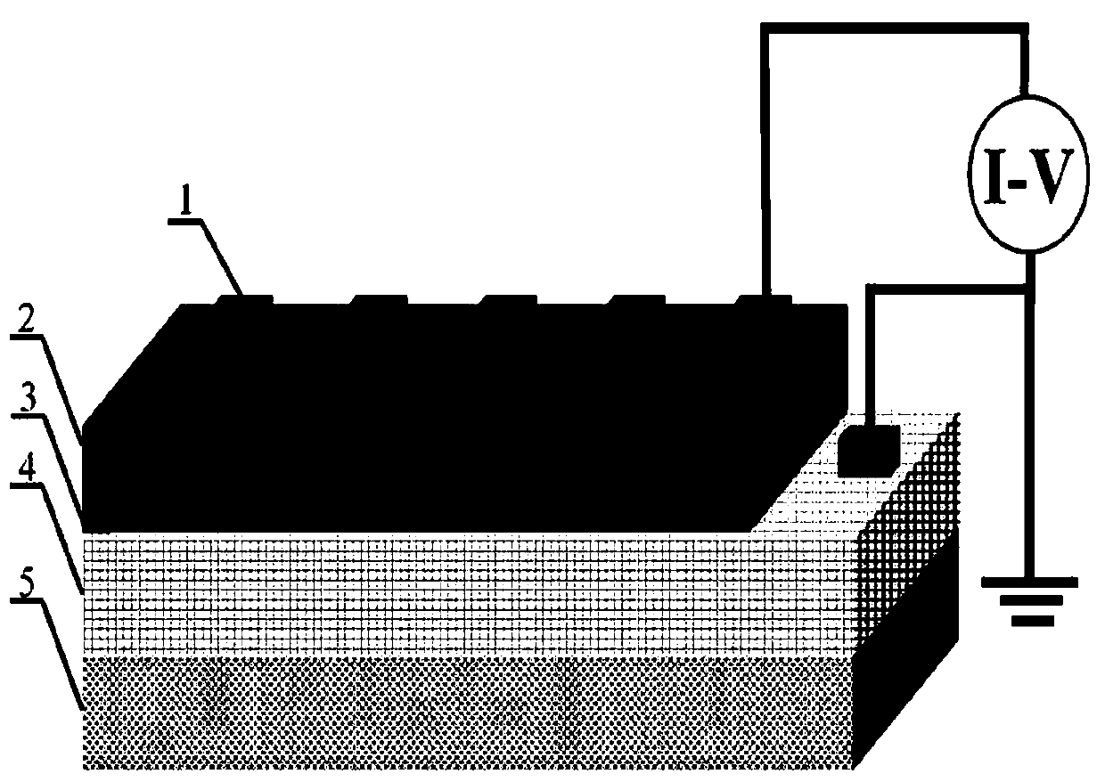
[0039] (1) With the clean silicon wafer 5 as the substrate, the lower electrode 4 is firstly prepared by plasma-enhanced atomic layer deposition, and the lower electrode TiN is prepared. The specific steps are as follows:

[0040] TiN growth temperature is 400°C, with TiCl 4 , NH 3 Plasma is used as Ti source and nitrogen source respectively, where TiCl 4 The pulse time is 0.1 seconds, the carrier gas is high-purity nitrogen (99.999%), and it is used as a cleaning gas at the same time, and the cleaning time is 4 seconds; NH 3 The carrier gas of the plasma is high-purity argon (99.999%), and its pulse time is 24 seconds. The cleaning time of high-purity nitrogen as the cleaning gas is 6 seconds. TiCl 4 The source temperature is room temperature. In this embodiment, the thickness of TiN is 30nm;

[0041] (2) CoPt was grown on the lower electrode TiN layer by plasma-enhanced atomic layer deposition x Magnetic nanocrystalline layer 3;

[0042] CoPt x The nanocrystal growth ...

Embodiment 2

[0053] (1) Using a clean silicon wafer as the substrate, firstly prepare the lower electrode TiN with a thickness of 120 nm by using plasma-enhanced atomic layer deposition, and the preparation method is the same as step (1) in Example 1;

[0054] (2) CoPt was grown on the lower electrode TiN layer by plasma-enhanced atomic layer deposition x Nanocrystals, the preparation method of which is the same as step (2) in Example 1, the cycle ratio of Co:Pt is 1:1, and the number of cycles is 100 cycles;

[0055] (3) Second, hafnium oxide thin film was grown to form the resistive switch layer. The atomic layer deposition process conditions were as follows: the growth temperature was 250°C, tetrakis-(dimethylethylamino hafnium) and secondary deionized water were used as Hf source and oxygen source respectively, each The pulse time of Luyuan is 0.1 seconds, the carrier gas is high-purity nitrogen (99.999%) and it is also used as cleaning gas, and the cleaning time is 4 seconds. Tetra-(...

Embodiment 3

[0063] (1) With a clean silicon wafer as the substrate, the lower electrode TiN was first prepared by plasma-enhanced atomic layer deposition. The specific steps are as follows:

[0064] TiN growth temperature is 400°C, with TiCl 4 , NH 3 Plasma is used as Ti source and nitrogen source respectively, where TiCl 4 The pulse time is 0.1 seconds, the carrier gas is high-purity nitrogen (99.999%), and it is used as a cleaning gas at the same time, and the cleaning time is 4 seconds; NH 3 The carrier gas of the plasma is high-purity argon (99.999%), and its pulse time is 24 seconds. The cleaning time of high-purity nitrogen as the cleaning gas is 6 seconds. TiCl 4 The source temperature is room temperature. In this embodiment, the thickness of TiN is 200nm;

[0065] (2) CoPt was grown on the lower electrode TiN layer by plasma-enhanced atomic layer deposition x nanocrystalline layer;

[0066] CoPt x The nanocrystal growth temperature was 300°C, and the PtMeCpMe 3 , CoCp(CO) ...


PUM

PropertyMeasurementUnit
diameteraaaaaaaaaa
thicknessaaaaaaaaaa
thicknessaaaaaaaaaa

Abstract

The invention discloses a CoPtx nano-composite structure electromagnetic storage device. The electromagnetic storage device is a stacked layer structure, and the stacked layers are sequentially composed of a silicon wafer, a lower electrode, a CoPtx magnetic nanocrystalline layer, and an oxide Thin-film resistive layer and upper electrode; the memory of the present invention has excellent resistive memory function and magnetic recording characteristics, and can realize high-density multi-state electromagnetic memory function; the present invention also discloses its preparation method, which is based on The multifunctional and high-density electromagnetic storage device preparation technology of atomic layer deposition has good compatibility with microelectronics technology, provides feasibility for future industrial scale application, and can guarantee the uniformity, conformality and Controllability, and compatibility with mature semiconductor technology, it is convenient to realize the integration of high-density multifunctional electromagnetic storage devices and microelectronic devices, and realize large-scale and industrial applications.

Description

technical field [0001] The invention belongs to the field of micro-nano electronic technology-high-density information storage, and relates to a CoPt x Electromagnetic storage device with nanocomposite structure and its preparation method. Background technique [0002] Flash memory based on charge storage mechanism, with the reduction of device size, it is difficult to break through the process bottleneck of the 22nm technology node, and cannot meet the rapid development of the information field. A new type of non-volatile memory device - resistive random access memory (RRAM) came into being. The information reading and writing of resistive memory devices is realized by reading or changing the resistance of resistive materials. Its functional layer has high resistance state and low resistance state, corresponding to two states of "0" and "1". Under the condition of external voltage, the resistive memory device can realize reversible switching between high and low resistanc...

Claims


Application Information

Patent Timeline
Patent Type & Authority Patents(China)
IPC IPC(8): G11C11/15H01L45/00
CPCG11C11/15H10B53/00
Inventor 李爱东王来国吴迪
Owner NANJING UNIV
Why Eureka
Try Eureka