

CoPtx nano composite structure electromagnetic memory device and preparation method thereof
A storage device and nano-composite technology, applied in the direction of static memory, electric solid device, digital memory information, etc., to achieve the effect of reducing randomness, guaranteeing conformity and controllability, and excellent storage performance
- Summary
- Abstract
- Description
- Claims
- Application Information
AI Technical Summary
Problems solved by technology
Method used
Image

Examples
Embodiment 1
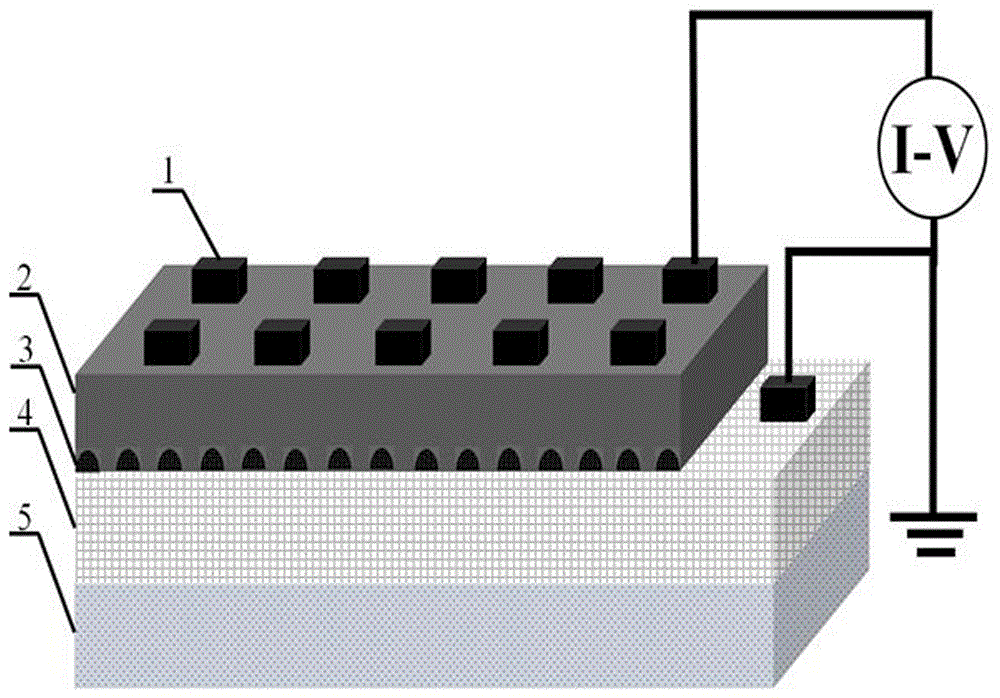
[0039] (1) With the clean silicon wafer 5 as the substrate, the lower electrode 4 is firstly prepared by plasma-enhanced atomic layer deposition, and the lower electrode TiN is prepared. The specific steps are as follows:
[0040] TiN growth temperature is 400°C, with TiCl 4 , NH 3 Plasma is used as Ti source and nitrogen source respectively, where TiCl 4 The pulse time is 0.1 seconds, the carrier gas is high-purity nitrogen (99.999%), and it is used as a cleaning gas at the same time, and the cleaning time is 4 seconds; NH 3 The carrier gas of the plasma is high-purity argon (99.999%), and its pulse time is 24 seconds. The cleaning time of high-purity nitrogen as the cleaning gas is 6 seconds. TiCl 4 The source temperature is room temperature. In this embodiment, the thickness of TiN is 30nm;
[0041] (2) CoPt was grown on the lower electrode TiN layer by plasma-enhanced atomic layer deposition x Magnetic nanocrystalline layer 3;
[0042] CoPt x The nanocrystal growth ...
Embodiment 2
[0053] (1) Using a clean silicon wafer as the substrate, firstly prepare the lower electrode TiN with a thickness of 120 nm by using plasma-enhanced atomic layer deposition, and the preparation method is the same as step (1) in Example 1;
[0054] (2) CoPt was grown on the lower electrode TiN layer by plasma-enhanced atomic layer deposition x Nanocrystals, the preparation method of which is the same as step (2) in Example 1, the cycle ratio of Co:Pt is 1:1, and the number of cycles is 100 cycles;
[0055] (3) Second, hafnium oxide thin film was grown to form the resistive switch layer. The atomic layer deposition process conditions were as follows: the growth temperature was 250°C, tetrakis-(dimethylethylamino hafnium) and secondary deionized water were used as Hf source and oxygen source respectively, each The pulse time of Luyuan is 0.1 seconds, the carrier gas is high-purity nitrogen (99.999%) and it is also used as cleaning gas, and the cleaning time is 4 seconds. Tetra-(...
Embodiment 3
[0063] (1) With a clean silicon wafer as the substrate, the lower electrode TiN was first prepared by plasma-enhanced atomic layer deposition. The specific steps are as follows:
[0064] TiN growth temperature is 400°C, with TiCl 4 , NH 3 Plasma is used as Ti source and nitrogen source respectively, where TiCl 4 The pulse time is 0.1 seconds, the carrier gas is high-purity nitrogen (99.999%), and it is used as a cleaning gas at the same time, and the cleaning time is 4 seconds; NH 3 The carrier gas of the plasma is high-purity argon (99.999%), and its pulse time is 24 seconds. The cleaning time of high-purity nitrogen as the cleaning gas is 6 seconds. TiCl 4 The source temperature is room temperature. In this embodiment, the thickness of TiN is 200nm;
[0065] (2) CoPt was grown on the lower electrode TiN layer by plasma-enhanced atomic layer deposition x nanocrystalline layer;
[0066] CoPt x The nanocrystal growth temperature was 300°C, and the PtMeCpMe 3 , CoCp(CO) ...
PUM
| Property | Measurement | Unit |
|---|---|---|
| Thickness | aaaaa | aaaaa |
| The average diameter | aaaaa | aaaaa |
| Thickness | aaaaa | aaaaa |
Abstract
Description
Claims
Application Information