Polycrystalline silicon thin film transistors with bridged-grain structures

A thin film transistor and transistor technology, applied in transistors, electric solid state devices, semiconductor devices, etc., can solve the problems of increased threshold voltage, total mobility loss, etc., and achieve the effect of reducing threshold voltage and leakage current, and improving uniformity

Inactive Publication Date: 2010-03-24
THE HONG KONG UNIV OF SCI & TECH
View PDF4 Cites 22 Cited by
  • Summary
  • Abstract
  • Description
  • Claims
  • Application Information

AI Technical Summary

Problems solved by technology

Conduction across grain boundaries is worse than inside the crystalline materi

Method used


Image

  • Polycrystalline silicon thin film transistors with bridged-grain structures
  • Polycrystalline silicon thin film transistors with bridged-grain structures
  • Polycrystalline silicon thin film transistors with bridged-grain structures

Examples


Embodiment Construction

[0052] The many innovative teachings of the present application will be described with particular reference to presently preferred embodiments, by way of example, and not limitation.

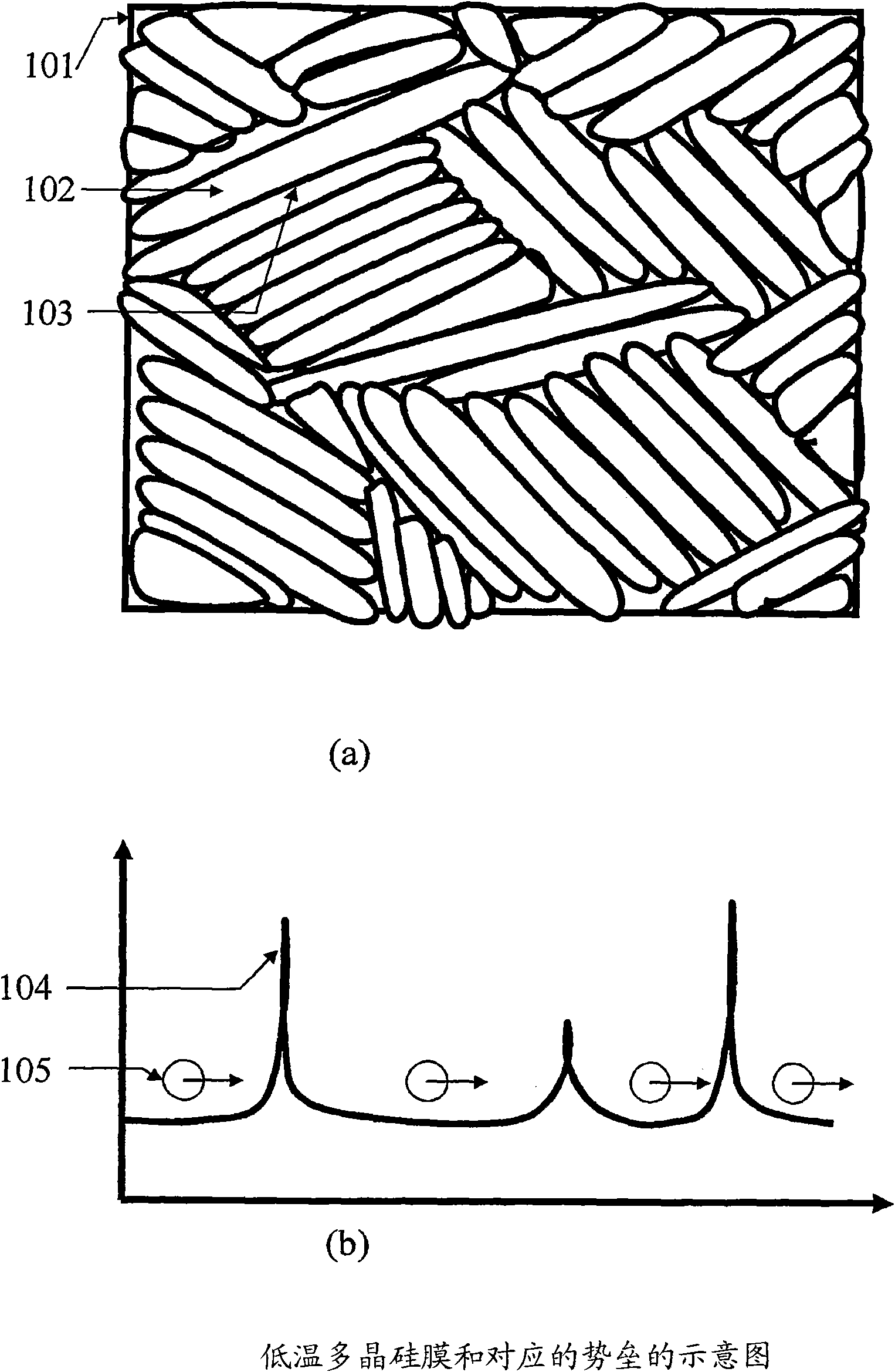
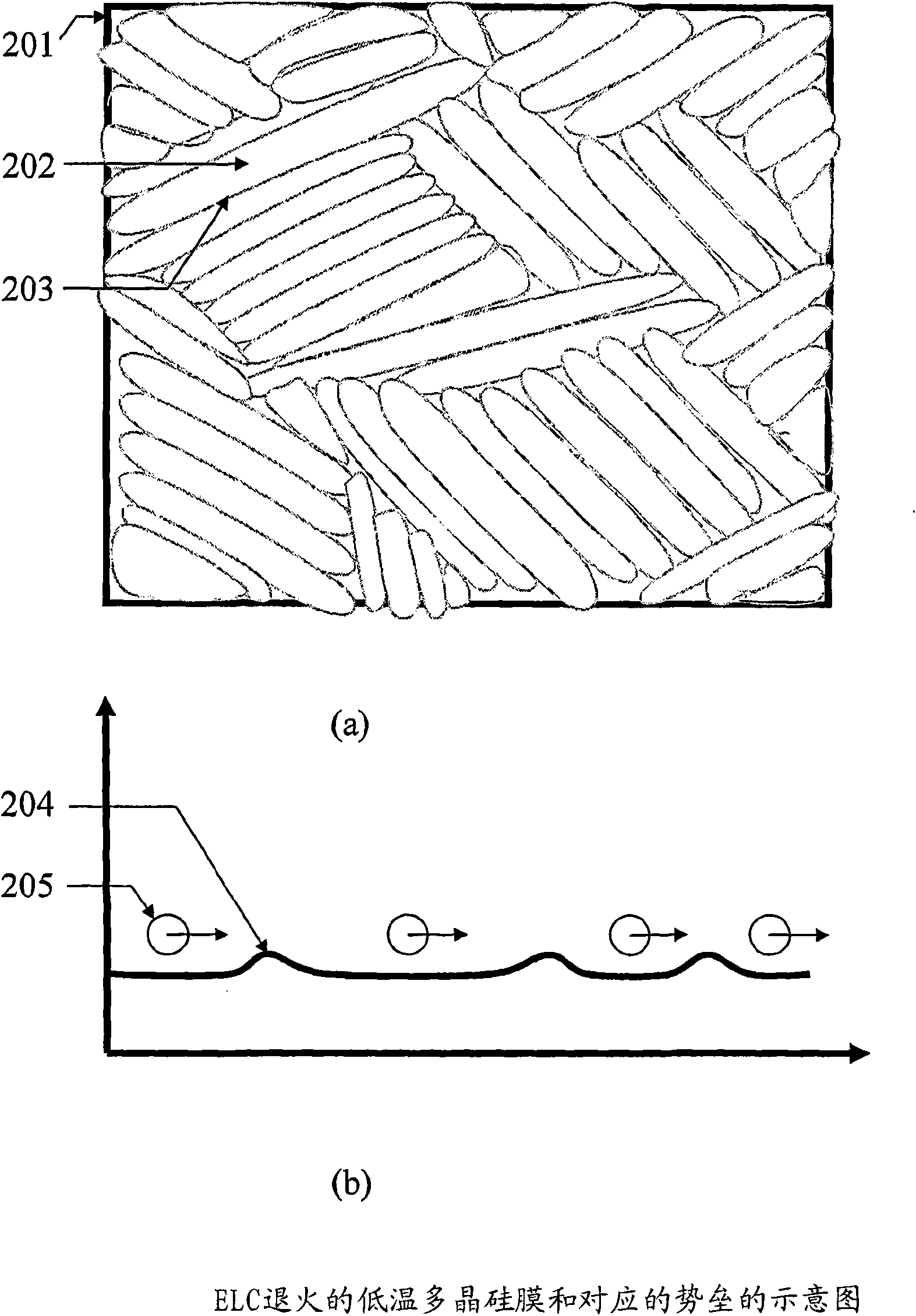
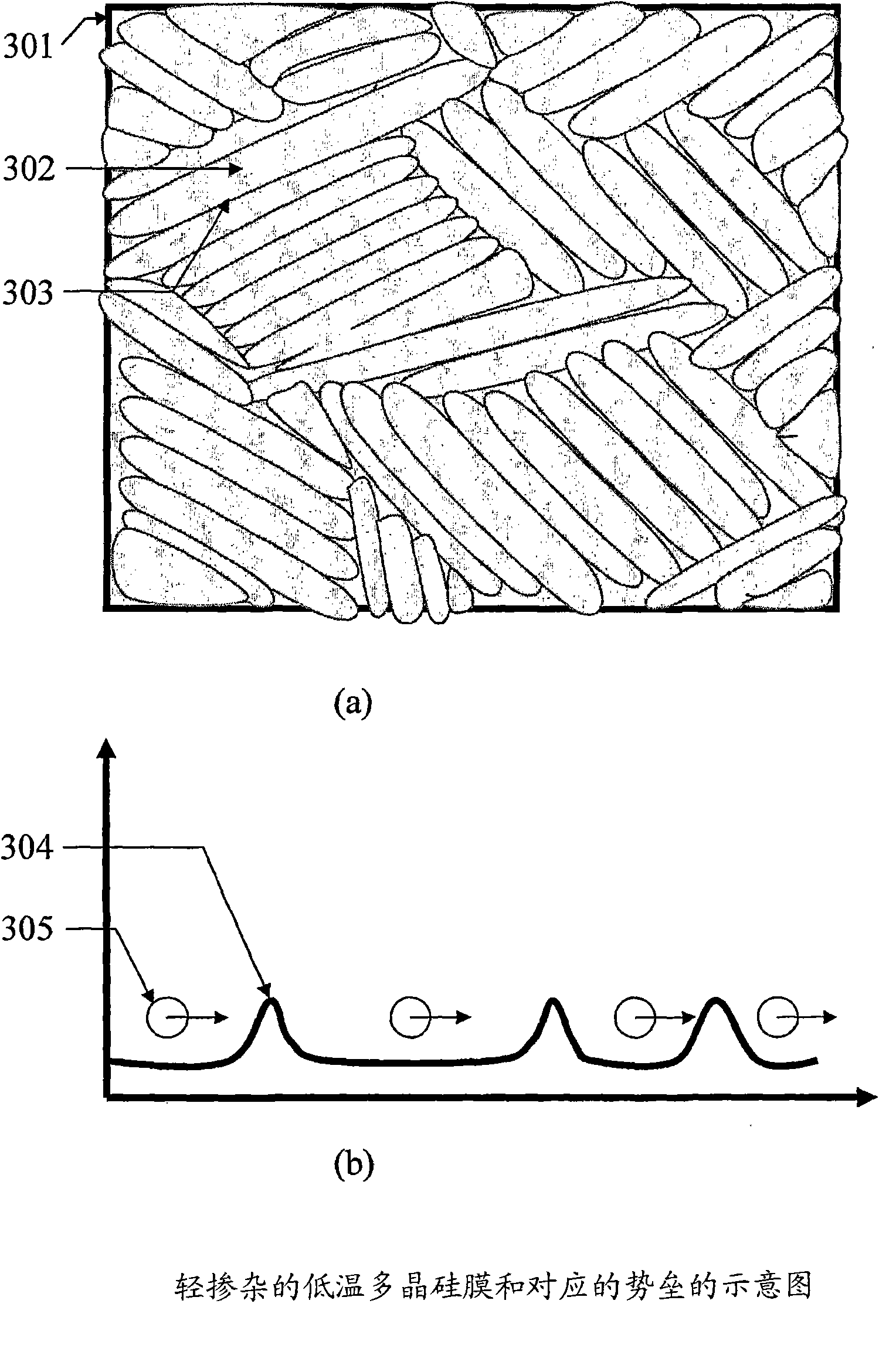
[0053] One of the disclosed inventions is to use conductive strips or bridges to connect the die inside the active channel of a TFT. The crystal grains are randomly distributed inside the channel, as shown in Figs. 1-3. The performance of the TFT can be greatly improved by forming conductive bands or lines between the crystal grains perpendicular to the direction of current movement. Basically the two-dimensional network is turned into a pseudo-one-dimensional network. Referring briefly to Figure 4a, the conductive wires facilitate the flow of current in a direction perpendicular to the current flow. The influence of grain boundaries is reduced by these conductive lines, which can be considered as bridges across the grains. This structure is defined as a bridge grain (BG) structure. However,...


PUM

PropertyMeasurementUnit
Widthaaaaaaaaaa

Abstract

A low temperature polycrystalline silicon device and techniques to manufacture thereof with excellent performance. Employing doped poly-Si lines which we called a bridged-grain structure (BG), the intrinsic or lightly doped channel is separated into multiple regions. A single gate covering the entire active channel including the doped lines is still used to control the current flow. Using this BGpoly-Si as an active layer and making sure the TFT is designed so that the current flows perpendicularly to the parallel lines of grains, grain boundary effects can be reduced. Reliability, uniformityand the electrical performance of the BG poly-Si TFT are significantly improved compared with the conventional low temperature poly-Si TFT.

Description

[0001] CROSS REFERENCE TO OTHER APPLICATIONS [0002] Priority is claimed to US provisional application 60 / 929,338, the entire contents of which are hereby incorporated by reference. technical field [0003] The present application relates to methods and systems for forming high performance, high uniformity, and high reliability low temperature polycrystalline thin film devices on glass substrates. Background technique [0004] The following paragraphs contain discussions that illuminate through the innovations disclosed in this application, and any discussion in these paragraphs of actual or proposed or possible approaches does not imply that those approaches are prior art. [0005] Display devices such as those used in televisions and computer screens are rapidly evolving into high-quality flat panel displays using active matrix drive technology. The latest display technologies, such as Liquid Crystal Displays (LCD), Organic Light Emitting Diodes (OLED), and Electronic In...

Claims


Application Information

Patent Timeline
IPC IPC(8): H01L29/786H01L21/38
CPCH01L27/1214H01L29/04H01L29/66757H01L29/78696H01L27/1281H01L29/78618
Inventor 郭海成王文孟志国赵淑云
Owner THE HONG KONG UNIV OF SCI & TECH
Why Eureka
Try Eureka