

Chemical mechanical grinding method
A chemical-mechanical and grinding method technology, applied in electrical components, semiconductor/solid-state device manufacturing, circuits, etc., can solve the problems of structural damage, influence, poor CMP process stability, etc., to improve the overall process uniformity, improve the good quality. rate effect
- Summary
- Abstract
- Description
- Claims
- Application Information
AI Technical Summary
Problems solved by technology
Method used
Image

Examples
Embodiment Construction
[0035] The following will clearly and completely describe the technical solutions in the embodiments of the present invention with reference to the accompanying drawings in the embodiments of the present invention. Obviously, the described embodiments are only some, not all, embodiments of the present invention. Based on the embodiments of the present invention, all other embodiments obtained by persons of ordinary skill in the art without making creative efforts belong to the protection scope of the present invention.
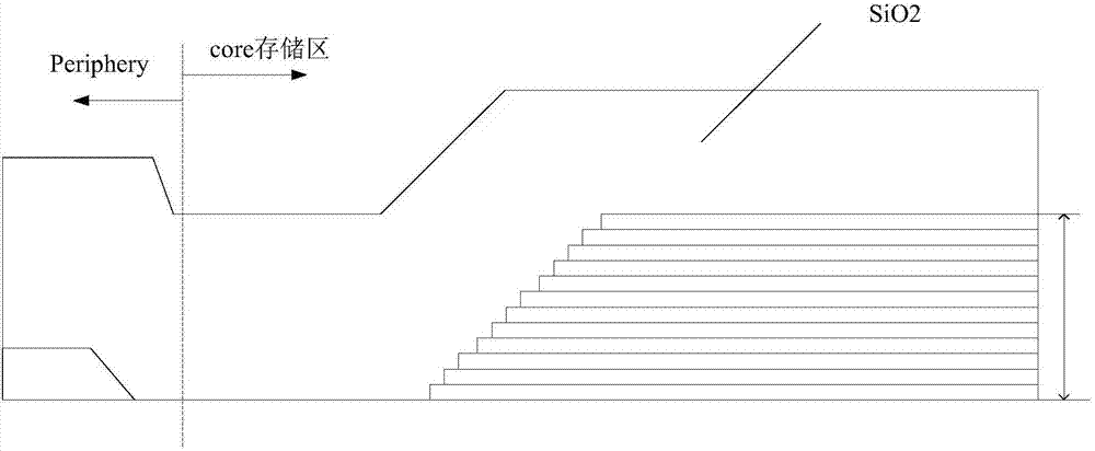
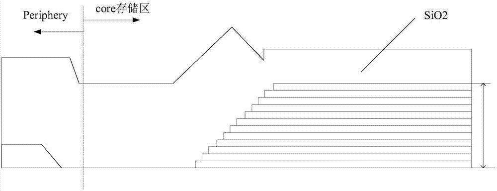
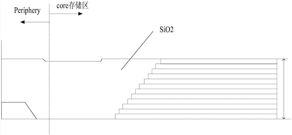
[0036] In the chemical mechanical polishing method provided by this solution, first, after depositing an oxide layer on the peripheral circuit region of the three-dimensional memory and the storage region, the first etching is performed on the peripheral circuit region, so that the oxide layer of the peripheral circuit region The lowest height is the same as the highest height of the steps in the storage area; and a barrier layer is formed on the oxide layer of...
PUM
 Abstract
Description
Claims
Application Information