Device array of silicon carbide gate turn-off thyristor GTO and preparation method thereof

Pending Publication Date: 2018-09-18
INST OF ELECTRONICS ENG CHINA ACAD OF ENG PHYSICS
View PDF0 Cites 5 Cited by
  • Summary
  • Abstract
  • Description
  • Claims
  • Application Information

AI Technical Summary

Problems solved by technology

These material defects have a significant negative impact on the withstand voltage capability of GTO devices
Due to the objective existence of material defects, no matter how the terminal structure design of large-scale devices is optimized, premature breakdown of devices caused by internal defect-assisted tunneling leakage is inevitable, which will significantly reduce the blocking voltage level of devices
However, in order to meet the requirements for the large current carrying capacity of

Method used


Image

  • Device array of silicon carbide gate turn-off thyristor GTO and preparation method thereof
  • Device array of silicon carbide gate turn-off thyristor GTO and preparation method thereof
  • Device array of silicon carbide gate turn-off thyristor GTO and preparation method thereof

Examples


Embodiment 1

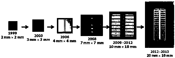
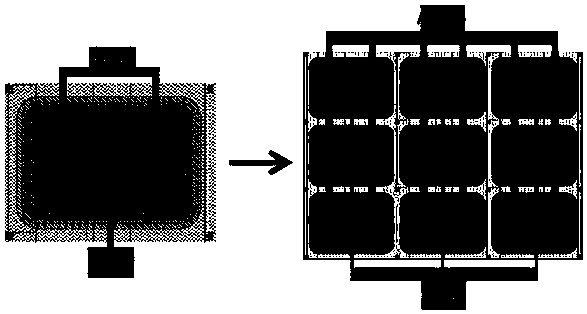
[0039] A silicon carbide gate turn-off thyristor device array (SiC GTO Array), the epitaxial structure of the SiC material is the P+ / N / P- / P / N+ structure in the SiC GTO device from top to bottom, from top to bottom Each epitaxial layer is a P+ contact layer in turn (doping concentration 2×10 19 cm -3 , thickness 2μm), N base layer (doping concentration 2.3×10 17 cm -3 , thickness 2μm), P-drift layer (doping concentration 2×10 14 cm -3 , thickness 60μm), P buffer layer (doping concentration 2×10 17 cm -3 , thickness 2μm), N+ field stop layer (doping concentration 2×10 18 cm -3 , thickness 1μm), the bottom is N+ 4H-SiC intrinsic substrate. The device unit mesa size of the SiC GTO device array is 3.52mm*2.52mm; the device array is an area array with 3 columns and 4 rows, which contains a total of 12 GTO devices, and the overall design size of the array is 11.46mm*11.28mm.

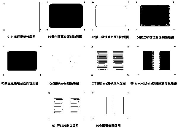
[0040] according to image 3 The photolithographic layout design in the present embodiment, the pr...

Embodiment 2

[0055] Another silicon carbide gate turn-off thyristor device array (SiC GTO Array), the epitaxial structure of its SiC material is a typical P+ / N / P- / P / N+ structure in SiC GTO devices from top to bottom, from top to bottom Each epitaxial layer to the next is the P+ contact layer (doping concentration 2×10 19 cm -3 , thickness 2μm), N base layer (doping concentration 2.3×10 17 cm -3 , thickness 2μm), P-drift layer (doping concentration 2×10 14 cm -3 , thickness 90μm), P buffer layer (doping concentration 2×10 17 cm -3 , thickness 2μm), N+ field stop layer (doping concentration 2×10 18 cm -3 , thickness 1μm), the bottom is N+ 4H-SiC intrinsic substrate. The device unit mesa size of the SiC GTO device array is 3.52mm*5.04mm; the device array is an area array with 6 columns and 4 rows, which contains a total of 24 GTO devices, and the overall design size of the array is 22.92mm*21.36mm.

[0056] The device array process preparation flow in embodiment 2 is similar to the p...


PUM

PropertyMeasurementUnit
Thicknessaaaaaaaaaa
Thicknessaaaaaaaaaa
Areaaaaaaaaaaa

Abstract

The invention provides a device array of a silicon carbide gate turn-off thyristor GTO and a preparation method thereof, wherein each single device is relatively small in size. The device array is formed by photoetching according to a corresponding photoetching layout and comprises at least two array structures of silicon carbide gate turn-off thyristors. The gate electrode of a GTO device unit islocated in the center of the table surface of the device unit. The gate electrode of the GTO device unit forms an interdigital structure together with anodes located on the two sides of the table surface of the device unit. A cathode is located on the back surface of the substrate of the device unit. During the packaging process, the gate electrodes of all device units are led down to a packagingstructure according to the layout design. Meanwhile, all anodes are led out in the opposite directions of the gate electrodes. According to the device array scheme adopted by the invention, the effective working area of a whole packaging chip can be remarkably improved. The condition that the performance of the whole packaging chip is reduced due to the defects of local materials can be avoided.Moreover, the process difficulty of device machining can be reduced, and the process stability and the process uniformity can be improved. The yield of prepared devices can be remarkably improved.

Description

technical field [0001] The invention relates to a silicon carbide gate turn-off thyristor GTO device array and a preparation method thereof, belonging to the technical field of semiconductor power electronic devices. Background technique [0002] Silicon carbide (SiC) material, as a new type of wide bandgap semiconductor material, has a series of excellent material properties. These characteristics include large band gap, high critical breakdown field strength, high electron saturation drift velocity, radiation resistance and normal operation at higher temperatures; in addition, the current epitaxial growth technology of silicon carbide materials is relatively It is also more mature than other common wide bandgap semiconductors. These factors together determine that SiC material is the preferred material for preparing various types of advanced power devices. [0003] Since the critical breakdown field strength of SiC is almost ten times that of Si, when preparing power dev...

Claims


Application Information

Patent Timeline
IPC IPC(8): H01L27/02H01L29/744H01L23/31H01L23/367
CPCH01L27/0207H01L29/744H01L23/3121H01L23/367Y02P70/50
Inventor 李良辉周坤徐星亮李俊焘李志强张林代刚
Owner INST OF ELECTRONICS ENG CHINA ACAD OF ENG PHYSICS
Why Eureka
Try Eureka