Method and system for predicting growth thickness of lead-free solder joint interface metal compound

A metal compound and metal compound layer technology, which is applied in the direction of testing metals, testing metal structures, measuring devices, etc., can solve the problem of inaccurate prediction results of the growth thickness of interfacial metal compounds

Active Publication Date: 2019-11-08
CHINA ELECTRONICS PROD RELIABILITY & ENVIRONMENTAL TESTING RES INST
View PDF3 Cites 0 Cited by
  • Summary
  • Abstract
  • Description
  • Claims
  • Application Information

AI Technical Summary

Problems solved by technology

[0003] Based on this, a prediction method for the growth thickness of interfacial metal compounds in lead-free solder joints is proposed to solve the problem of inaccurate prediction results of interfacial metal compound growth thickness

Method used


Image

  • Method and system for predicting growth thickness of lead-free solder joint interface metal compound
  • Method and system for predicting growth thickness of lead-free solder joint interface metal compound
  • Method and system for predicting growth thickness of lead-free solder joint interface metal compound

Examples


Embodiment Construction

[0023] In order to further explain the technical means adopted by the present invention and the effects obtained, the technical solutions of the embodiments of the present invention will be clearly and completely described below in conjunction with the accompanying drawings and preferred embodiments.

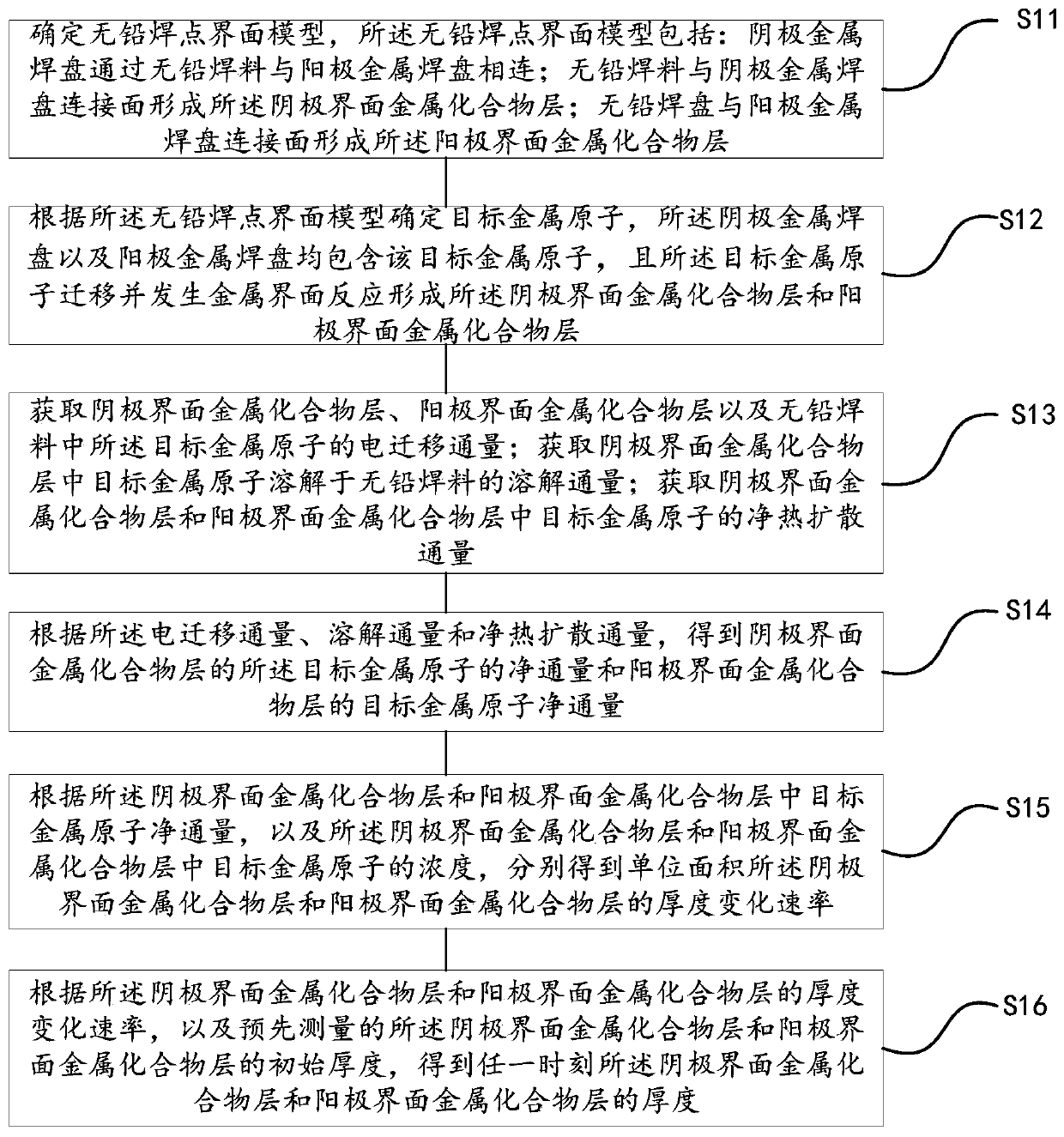
[0024] figure 1 It is a schematic flow chart of the prediction method for the growth thickness of metal compounds at the interface of lead-free solder joints, as shown in figure 1 As shown, the prediction method of the growth thickness of the lead-free solder joint interface metal compound in this embodiment includes the following steps:

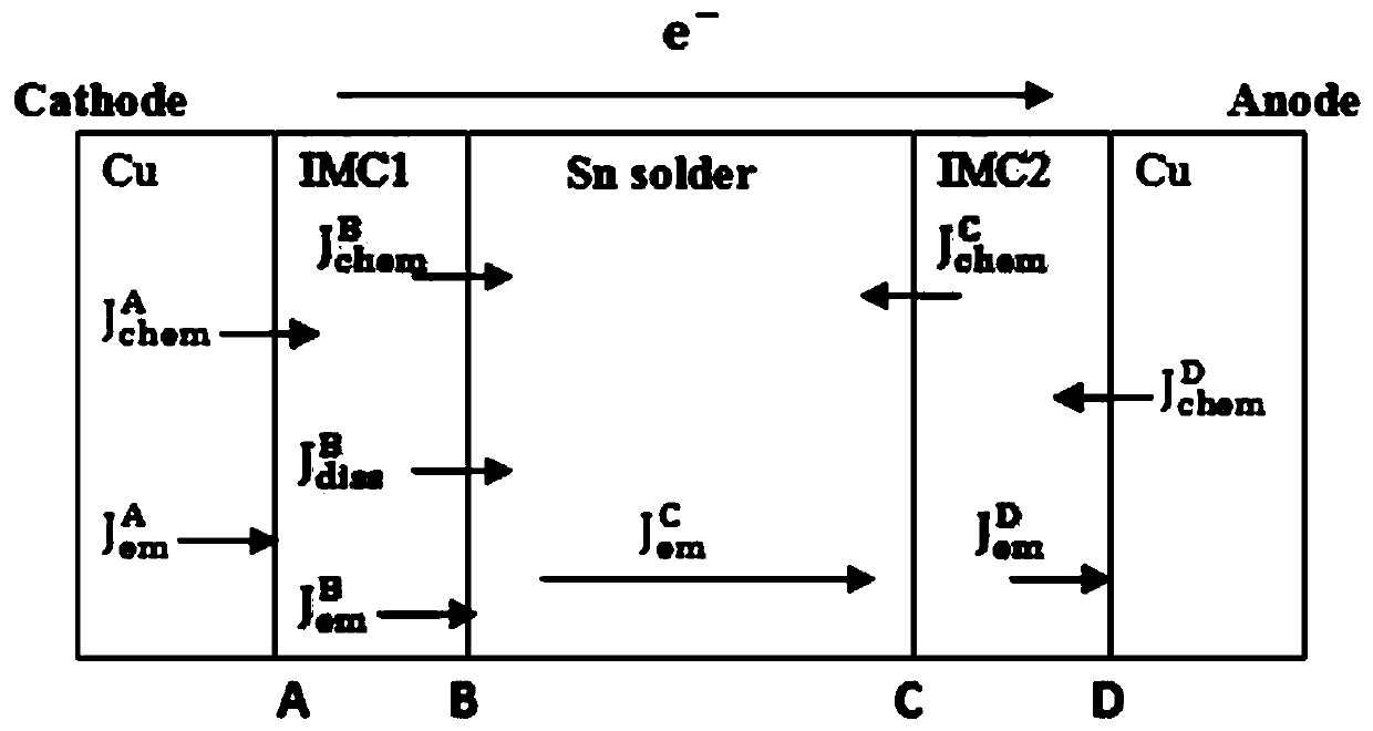
[0025] S11, determine the lead-free solder joint interface model, the lead-free solder joint interface model includes: the cathode metal pad is connected to the anode metal pad through lead-free solder; the connection surface of the lead-free solder and the cathode metal pad forms the cathode interface Metal compound layer; the connection sur...


PUM


Abstract

The invention relates to a leadless solder joint interface metallic compound growth thickness prediction method and a system thereof. The method comprises the following steps: determining a leadless solder joint interface model and a target metal atom, obtaining the electromigration flux, dissolving flux and net-heat diffusion flux, calculating the thickness change rate of a cathode interface metallic compound layer and an anode interface metallic compound layer, according to the thickness change rate and initial thickness, obtaining the thickness of the cathode interface metallic compound layer and the anode interface metallic compound layer at any time. The above method can accurately predict the growth thickness of the interface metallic compound layer.

Description

technical field [0001] The invention relates to the field of electronic packaging, in particular to a method for predicting the growth thickness of a lead-free solder joint interface metal compound. Background technique [0002] In the future, electronic products will continue to be lead-free and miniaturized, and the influence of the intermetallic compound (IMC, intermetallic compound) layer on the reliability of solder joint interconnection becomes significant. During the use of the device, the solder IMC layer will grow slowly under the influence of temperature and time. And as the size of the solder joint shrinks, the volume ratio of the IMC layer in the interconnect solder joint increases greatly. Since the IMC layer is a brittle metallographic structure, it will greatly affect the service life of the solder joint. In recent years, however, the current method for predicting the growth thickness of the IMC layer in lead-free solder still has the problems of imperfect ba...

Claims


Application Information

Patent Timeline
Patent Type & Authority Patents(China)
IPC IPC(8): G01N13/00G01N25/00G01N33/204
CPCG01N13/00G01N25/00G01N33/20
Inventor 周斌付志伟李勋平何小琦
Owner CHINA ELECTRONICS PROD RELIABILITY & ENVIRONMENTAL TESTING RES INST
Why Eureka
Try Eureka