Leadless solder joint interface metallic compound growth thickness prediction method and system thereof
A metal compound and metal compound layer technology, which is applied in the direction of testing metals, measuring devices, surface/boundary effects, etc., can solve the problem of inaccurate prediction results of the growth thickness of interfacial metal compounds
- Summary
- Abstract
- Description
- Claims
- Application Information
AI Technical Summary
Problems solved by technology
Method used
Image
Examples
Embodiment Construction
[0023] In order to further explain the technical means adopted by the present invention and the effects obtained, the technical solutions of the embodiments of the present invention will be clearly and completely described below in conjunction with the accompanying drawings and preferred embodiments.
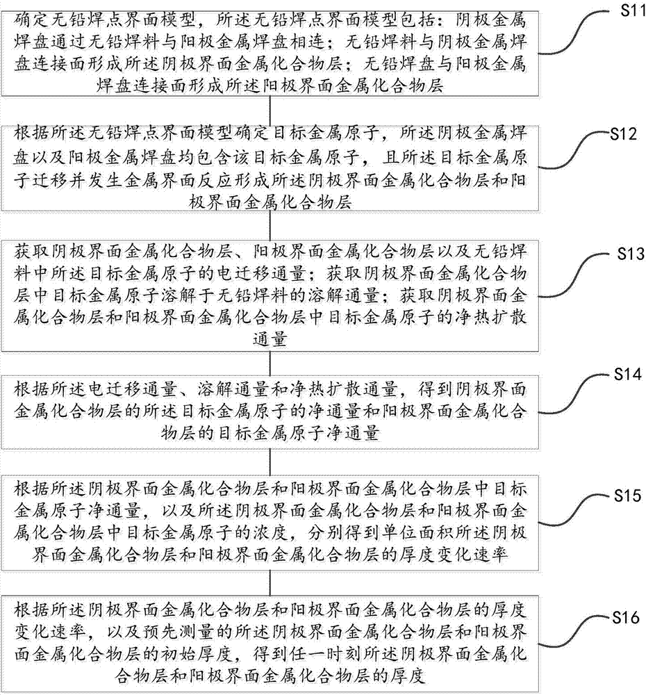
[0024] figure 1 It is a schematic flow chart of the prediction method for the growth thickness of metal compounds at the interface of lead-free solder joints, as shown in figure 1 As shown, the prediction method of the growth thickness of the lead-free solder joint interface metal compound in this embodiment includes the following steps:
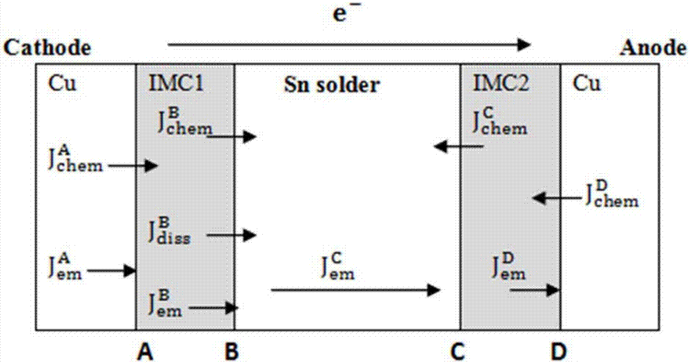
[0025] S11, determine the lead-free solder joint interface model, the lead-free solder joint interface model includes: the cathode metal pad is connected to the anode metal pad through lead-free solder; the connection surface of the lead-free solder and the cathode metal pad forms the cathode interface Metal compound layer; the connection sur...
PUM
 Abstract
Description
Claims
Application Information


